Electronics » Voltage Regulators and Power Supplies » Isolated DC-DC Power Modules »
5V, 300mA Isolated Step-Down Voltage Regulator D24Z3F5
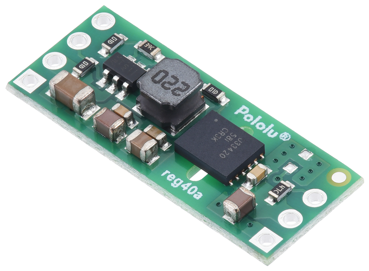
This step-down voltage regulator consists of an input step-down (buck) regulator in front of an isolated DC-to-DC power module. This enables up to 300 mA at 5 V (default) or 5.5 V (selectable) out from a wide 5.5 V to 36 V input.
| Input voltage | Output voltages | Max continuous output current | Size |
|---|---|---|---|
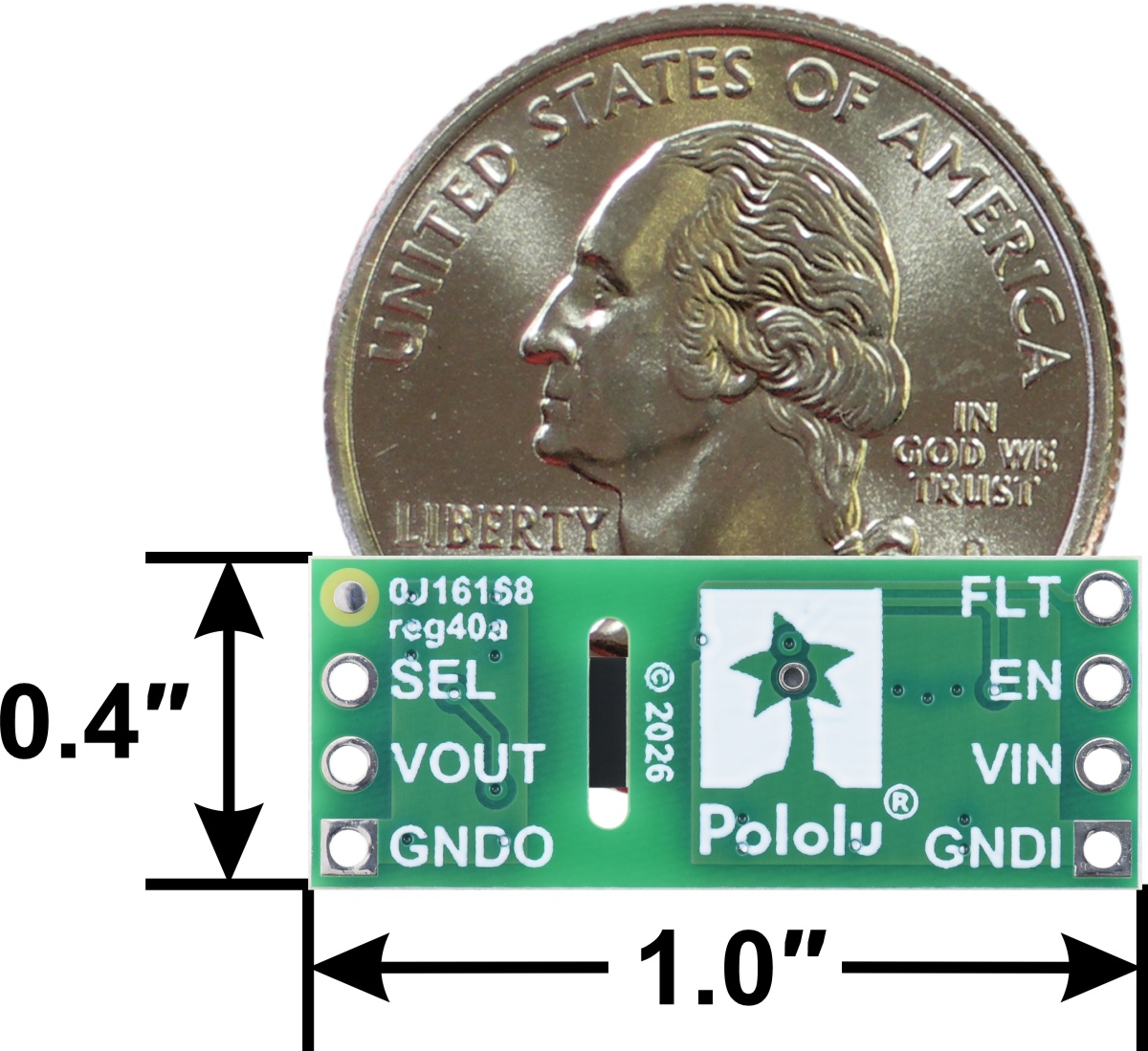
| 5.5 V to 36 V | 5 V (default) or 5.5 V (selectable) | 300 mA | 0.4″ × 1.0″ |
 Compare all products in Isolated DC-DC Power Modules or Step-Down (Buck) Voltage Regulators.
| Description | Specs (12) | Pictures (11) | Resources (4) | FAQs (0) | On the blog (0) | Distributors (5) |
|---|
Overview
This step-down voltage regulator consists of a 5 V buck regulator on the input side followed by a Texas Instruments UCC33420RAQR isolated DC-to-DC power module on the output side, enabling up to 300 mA at 5 V (default) or 5.5 V (selectable) out from a wide 5.5 V to 36 V input. Unlike non-isolated regulators, the output ground (GNDO) is effectively independent of the input side (GNDI), which can be useful for preventing ground loops and avoiding ground currents that can cause unpredictable system behavior or even lead to damage to potentially expensive components.
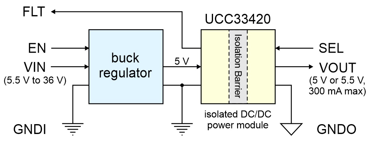 |
Block diagram of the 5V, 300mA Isolated Step-Down Voltage Regulator D24Z3F5. |
|---|
Here are some of the regulator’s key features:
 |
- Input voltage: 5.5 V to 36 V (can operate down to 4.6 V with reduced output current capabilities)
- Output voltage: 5 V (default) or 5.5 V (selectable) with 4% accuracy
- Output current: up to 300 mA continuous
- Galvanic isolation between input and output using the Texas Instruments UCC33420, which has the following isolation ratings:
- 3000 VRMS basic isolation rating
- 820 VRMS maximum working isolation voltage
- See the UCC33420 datasheet for more information
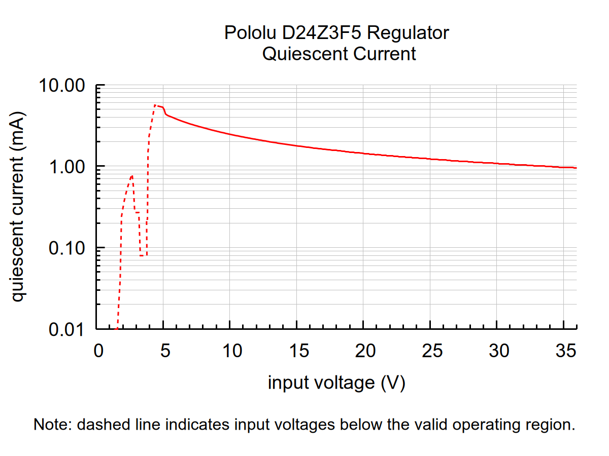
- Typical no-load quiescent current: 1 mA to 6 mA (see the quiescent current graph below)
- Typical efficiency: 45% to 55%, depending on input voltage and load (see efficiency graph below)
- Input (buck) switching frequency: ~1.1 MHz under heavy loads
- Output (isolated DC-DC converter) switching frequency: 64.5 MHz
- Input switching frequency decreases at low currents to improve light-load efficiency
- Over-temperature protection
- Size: 0.4″ × 1.0″ with breadboard-compatible, 0.1″-pitch through holes
The board does not have built-in protection against reverse voltage, but reverse-voltage protection modules are available for adding that functionality.
Using the module
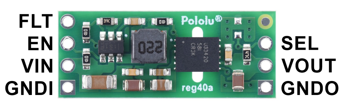 |
| Side | Pin | Description |
|---|---|---|
| Input | VIN | Input power supply. 5.5 V to 36 V should be supplied to this pin, though the device will operate down to around 4.6 V with reduced current capabilities. |
| GNDI | Ground connection for VIN. GNDI is NOT connected to GNDO. | |
| FLT | UCC33420 fault output. This connects directly to the FLT pin on the input side of the UCC33420 and is pulled up to input-side 5V through a 100 kΩ resistor. It drives low for 200 µs if an output under-voltage or thermal protection fault occurs on the UCC33420. | |
| EN | Enable input. This pin is pulled to VIN through a 100 kΩ resistor to enable the regulator by default. It can be driven low to put the board in a low-power state where the shut-down current is approximately equal to the current through the pull-up resistor (i.e. 10 µA per volt on VIN). | |
| Output | SEL | This pin provides direct access to the SEL input pin on the UCC33420, which determines the output voltage level, VOUT. It is pulled up to VOUT through a 30.1 kΩ resistor, which sets the output voltage to 5 V by default. Connect this pin to GNDO to select 5.5 V for the output. Note: The VOUT level is latched at power-up, so changing the SEL state while the board is powered will not have any effect until the regulator is power-cycled or EN is toggled. |
| VOUT | This pin provides direct access to the UCC33420 isolated VCC output. It is 5 V by default, and can optionally be set to 5.5 V using the SEL input as described above. | |
| GNDO | Ground connection for VOUT. GNDO is NOT connected to GNDI. |
The connections are labeled on the back side of the PCB and are arranged with a 0.1″ spacing along the edges of the board for compatibility with solderless breadboards, connectors, and other prototyping arrangements that use a 0.1″ grid. You can solder wires or 0.1″ header pins directly to the board. Note: header pins are not included with this product, but straight and right-angle male headers are available separately.
Typical efficiency
The efficiency of a voltage regulator, defined as (Power out)/(Power in), is an important measure of its performance, especially when battery life or heat are concerns. The graph below shows the efficiencies of the VOUT (5 V) output at different input voltages as a function of output current:
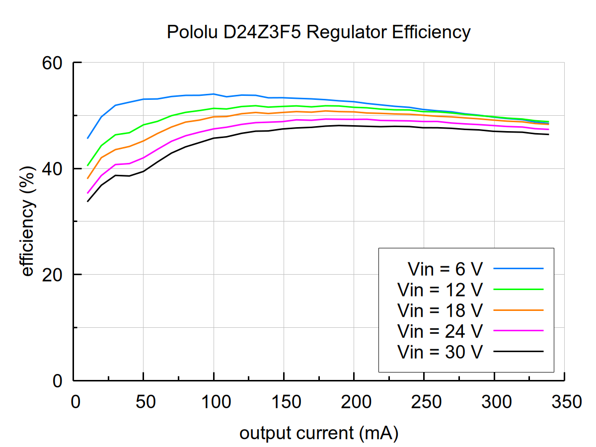 |
Please note that as this module consists of two chained regulators and includes isolated power transfer, the efficiency is below 60%, which is much lower than our non-isolated switching voltage regulators.
Maximum continuous output current
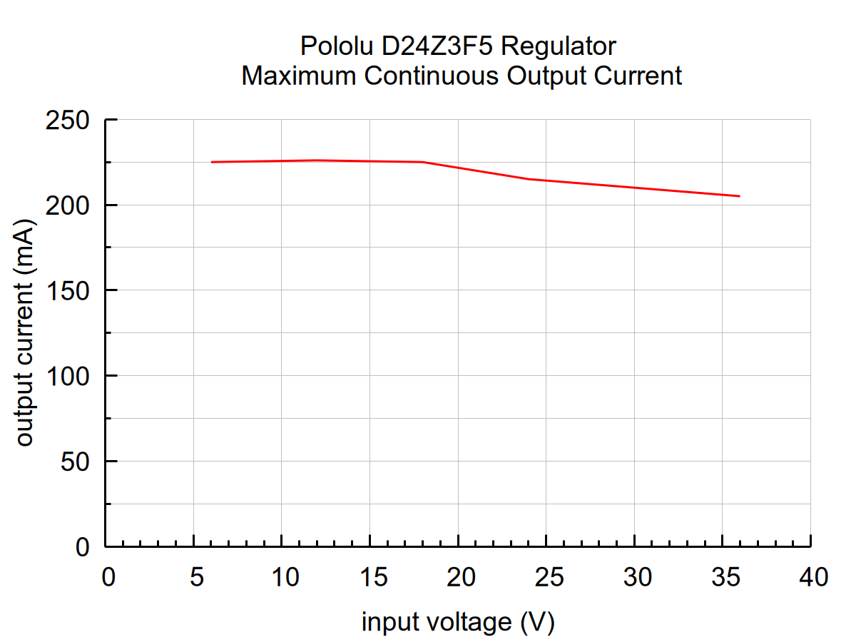
The UCC33420 is rated for up to 300 mA out continuous, and in our tests of the D24Z3F5 at room temperature and without forced airflow, the UCC33420 was able to sustain 300 mA continuously or for several minutes across most of the operating voltage range without the thermal shutdown activating. However, under those conditions, the temperature will exceed 125°C, so the following graph shows the continuous currents it can deliver without exceeding 125°C to allow better direct comparison with our other regulators. Slight heat sinking or forced airflow should be sufficient to achieve 300 mA continuous across the full operating voltage range.
 |
During normal operation, this product can get hot enough to burn you. Take care when handling this product or other components connected to it.
Quiescent current
The quiescent current is the current the regulator uses just to power itself. The graph below shows this as a function of the input voltage, including voltages outside the valid operating range of the device:
 |
Reduced output current for input voltages under 5.5 V
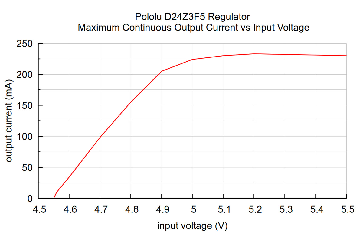
The recommended minimum input voltage for this regulator is 5.5 V, but it can operate down to around 4.6 V with reduced output current capabilities as shown in the graph below:
 |
Isolation rating and board creepage considerations
The UCC33420 provides basic isolation with a manufacturer-rated working voltage of 820 VRMS. The IC package has a clearance and creepage of >4.1 mm, and our PCB has a routed slot under the IC to provide a PCB creepage distance of 4.9 mm. A rough rule of thumb is that uncontaminated FR4 PCBs should have roughly 1 mm of creepage per 100 VRMS of isolation. Please note that our regulator module is not certified to any particular safety standard.
LC voltage spikes
When connecting voltage to electronic circuits, the initial rush of current can cause voltage spikes that are much higher than the input voltage. If these spikes exceed the regulator’s maximum voltage (36 V), the regulator can be destroyed. In our tests with typical power leads (~30″ test clips), we observed spikes approaching 36 V at input voltages approaching 20 V. Power supplies or leads with high inductance will make these spikes worse. An electrolytic capacitor (33 μF is a good starting point) can be added close to the regulator between VIN and GNDI to help suppress these spikes.
More information about LC spikes can be found in our application note, Understanding Destructive LC Voltage Spikes.
Related products


Related categories


Home | Forum | Blog | Support | Ordering Information | Lists | Distributors | BIG Order Form | About | Contact
© 2001–2026 Pololu Corporation