Overview
The D42V110Fx family of synchronous buck (step-down) voltage regulators generates lower output voltages from input voltages as high as 60 V. They are switching regulators (also called switched-mode power supplies (SMPS) or DC-to-DC converters), which makes them much more efficient than linear voltage regulators, especially when the difference between the input and output voltage is large. These regulators can typically support continuous output currents between 6 A and 16 A, depending on the input voltage and output voltage (see the Maximum continuous output current section below). In general, the available output current is higher for the lower-voltage versions than it is for the higher-voltage versions, and it decreases as the input voltage increases.
This family includes 11 versions with fixed output voltages ranging from 3.3 V to 24 V:
The regulators have input reverse voltage protection and over-current protection. A thermal shutdown feature also helps prevent damage from overheating and a soft-start feature limits the inrush current and gradually ramps the output voltage on startup.
We manufacture these boards in-house at our Las Vegas facility, so we can make these regulators with customized components to better meet the needs of your project, such as by customizing the output voltage. If you are interested in customization, please contact us.
For lower-power applications, consider the similar D42V55Fx step-down voltage regulators, which also operate from input voltages up to 60 V and can deliver approximately half as much current as the D42V110Fx.
Details for item #5677
|
|
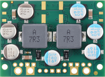 | 12V, 9A Step-Down Voltage Regulator D42V110F12, top view. |
|---|
|
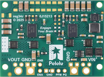 | 12V, 9A Step-Down Voltage Regulator D42V110F12, bottom view. |
|---|
|
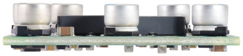 |
Side view of the Step-Down Voltage Regulator D42V110Fx (versions with output voltages of 12V or lower). |
|---|
Features
- Input voltage: 12 V to 60 V (minimum input subject to dropout voltage considerations; see the dropout voltage section for details)
- Output voltage: 12 V with 3% accuracy
- Typical maximum continuous output current: 6 A to 12 A (see the maximum continuous output current graph below)
- Typical efficiency >90%, depending on input voltage and load (see the efficiency graph below)
- Switching frequency: ~800 kHz under heavy loads
- < 0.3 mA typical no-load quiescent current (see the quiescent current graph below)
- Optional enable input for disconnecting the load and putting the regulator into a low-power state that typically draws under 0.2 mA
- Power-good output can be used for sequencing, fault detection, and voltage monitoring
- Soft-start feature limits inrush current and gradually ramps output voltage
- Integrated reverse-voltage protection, over-current protection, and over-temperature shutoff
- Compact size: 1.25″ × 1.7″ × 0.355″ (31.8 mm × 43.2 mm × 9 mm)
- Four 0.086″ mounting holes for #2 or M2 screws
Typical efficiency
The efficiency of a voltage regulator, defined as (Power out)/(Power in), is an important measure of its performance, especially when battery life or heat are concerns.
Connections
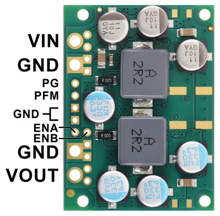 |
| Pin |
Type |
Function |
| VIN |
input |
Input power for the regulator. Voltages between 3.5 V and 60 V can be applied to VIN, but generally the effective lower limit of VIN is VOUT plus the regulator’s dropout voltage, which varies with the load (see below for graphs of the dropout voltage as a function of the load). |
| GND |
– |
Ground. All grounds on the board are common. |
| PG |
open-drain output |
Optional “Power Good” indicator that goes low when the regulator’s output voltage either rises more than 10% above or falls more than 8% below the nominal voltage (typical, with hysteresis). It drives low during soft start and while the regulator is disabled. An external pull-up resistor to the desired logic voltage rail is required to use this pin (100 kΩ recommended). |
| PFM |
input |
Optional input for selecting PFM or FPWM mode. Pin is pulled up to an internal 5V/3.3V voltage rail through a 100 kΩ resistor to select PFM mode by default, which dynamically reduces the switching frequency to improve light-load efficiency. Drive this pin low to select FPWM mode, which maintains a constant switching frequency independent of load. |
| ENA |
input |
Optional enable input for disconnecting the load and putting the regulator into a low-power shutdown mode that draws approximately 100 µA plus 2 µA per volt on VIN (note: this shutdown current draw can exceed the quiescent current draw of the regulator). This pin is pulled up to VIN by through a 1 MΩ resistor to enable the regulator by default, and it can be driven low to disable the regulator. |
| ENB |
input |
Optional input for disabling the secondary phase of the regulator to improve efficiency when powering light loads in FPWM mode. This pin should NOT be used when the regulator is operating in the default PFM mode. It is pulled up to VIN through a 1 MΩ resistor and connected to ENA through a 10 kΩ resistor. To use this feature, drive ENB low and drive ENA high (between 2 V and 5 V) while the board is in FPWM mode (PFM = low). When the secondary phase is disabled, the switching frequency reduces to ~400 kHz and the current output capabilities of the regulator are reduced by approximately 50%. |
| VOUT |
output |
Regulated output voltage. |
The board offers several options for making electrical connections. The three sets of smaller through-holes are arranged with a 0.1″ spacing for compatibility with solderless breadboards and 0.1″-pitch headers. The pairs of larger holes for VIN, VOUT, and GND are sized to accommodate 14 AWG wires or 2-pin 5mm-pitch terminal blocks.
The board has four 0.086″ mounting holes intended for #2 or M2 screws. The mounting holes are in the four corners of the board and are separated by 1.53″ horizontally and 1″ vertically. For all the board dimensions, see the dimension diagram (345k pdf).
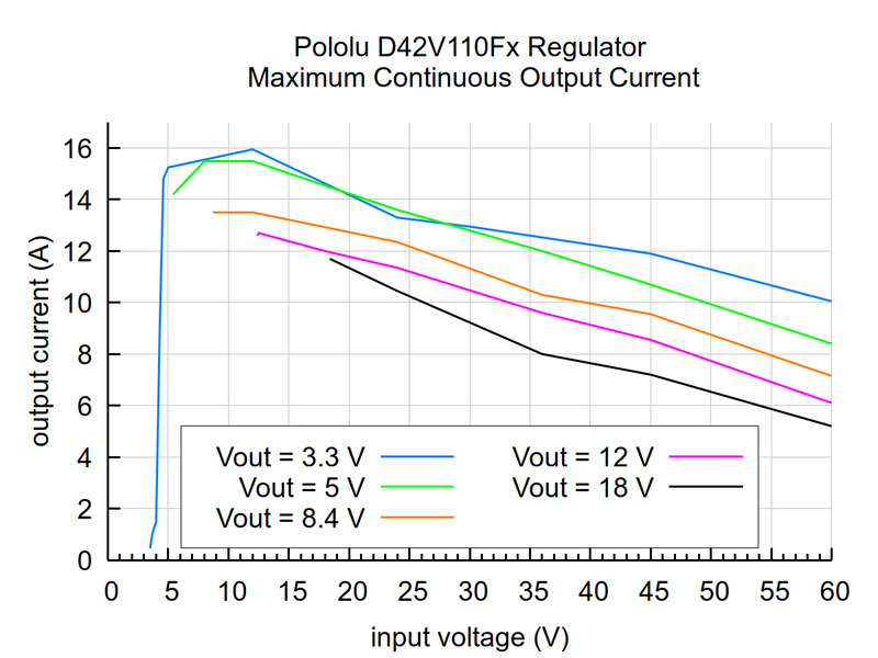
Maximum continuous output current
The maximum achievable output current of these regulators varies with the input voltage but also depends on other factors, including the ambient temperature, air flow, and heat sinking. The graph below shows maximum output currents that these regulators can deliver continuously at room temperature in still air and without additional heat sinking.
 |
During normal operation, this product can get hot enough to burn you. Take care when handling this product or other components connected to it.
This regulator has a protection feature that gracefully limits the output current, which can help protect it from thermal damage in applications loads that exceed the regulator’s capabilities. However, this limiting is insufficient to cover all possible combinations of input voltage, output voltage, and load, so we recommend you take precautions to ensure that the continuously applied loads of your application will not exceed the currents shown in the above graph. If your application has the potential to expose the regulator to higher loads, please consider using additional external protective components such as fuses or circuit breakers.
Quiescent current
The quiescent current is the current the regulator uses just to power itself, and the graph below shows this for the different regulator versions as a function of the input voltage. The module’s ENA input can be driven low to put the board into a low-power state where it draws approximately 100 µA plus 2 µA per volt on VIN (note that for high input voltages, this current draw can exceed the quiescent current draw of the regulator).
Typical dropout voltage
The dropout voltage of a step-down regulator is the minimum amount by which the input voltage must exceed the regulator’s target output voltage in order to ensure the target output can be achieved. For example, if a 5 V regulator has a 1 V dropout voltage, the input must be at least 6 V to ensure the output is the full 5 V. Generally speaking, the dropout voltage increases as the output current increases. The two graphs below shows the dropout voltages for this family (the 3.3 V version has its own separate graph because its dropout voltage curve is very different from the other members of this family):

 Compare all products in D42V110Fx Step-Down Voltage Regulators.


