Voltage Regulators and Power Supplies » Step-Up (Boost) Voltage Regulators » U3V40x Step-Up Voltage Regulators »
7.5V Step-Up Voltage Regulator U3V40F7

| Output voltage | Typical max input current* | Min input voltage |
|---|---|---|
| 7.5 V | 4 A | 1.3 V (2.7 V startup) |
*Actual achievable maximum continuous current is a function of input voltage and is limited by thermal dissipation. See the output current graphs on the product pages for more information.
Alternatives available with variations in these parameter(s): output voltage Select variant…

| Description | Specs (9) | Pictures (11) | Resources (3) | FAQs (0) | On the blog (0) | Distributors (49) |
|---|
Overview
 |
The U3V40Fx family of boost (step-up) voltage regulators are high-efficiency synchronous switching regulators that generate higher output voltages from input voltages as low as 1.3 V. (Note: minimum start-up voltage is 2.7 V; see the connections section for details.) The regulators actively limit the instantaneous input currents to 9.5 A while boosting, and the input current can typically be as high as 4.5 A for several seconds before the thermal protection activates. Input currents of around 3.5 A can typically be maintained for many minutes without triggering thermal shutdown, though the actual performance depends on the input and output voltages as well as external factors such as ambient temperature and airflow. For boost regulators, the output current equals the input current times the efficiency divided by the boost ratio of VOUT to VIN, so the more you are boosting, the lower the maximum output current will be (see the maximum continuous output current section below for performance graphs).
These regulators feature a variety of built-in protections, including cycle-by-cycle input current limiting, soft-start, configurable under-voltage lockout, and over-temperature shutdown.
Warning: This boost regulator uses the typical topology that connects the input to the output through an inductor and diode, with nothing to completely break that current path. Therefore, the input voltage will go through to the output when the regulator is disabled or when it exceeds the set output voltage, and exposure to short circuits or other excessive loads will damage the regulator. This regulator also does not have built-in protection against reverse voltage, but reverse-voltage protection modules are available for adding that functionality.
The U3V40x family includes five versions with fixed output voltages ranging from 5 V to 12 V.
- U3V40F5: Fixed 5V output
- U3V40F6: Fixed 6V output
- U3V40F7: Fixed 7.5V output
- U3V40F9: Fixed 9V output
- U3V40F12: Fixed 12V output
The different versions of the board all look very similar, so the bottom silkscreen includes a blank space where you can add your own distinguishing marks or labels.
We manufacture these boards in-house at our Las Vegas facility, so we can make these regulators with customized components to better meet the needs of your project, such as by customizing the output voltage between 2.7 V and 16 V. If you are interested in customization, please contact us.
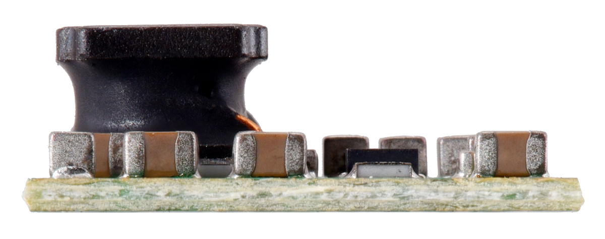 |
Step-Up Voltage Regulator U3V40Fx, side view. |
|---|
Details for item #4014
Features and specifications
- Output voltage: 7.5 V with 4% accuracy
- Input voltage: 1.3 V to 7.5 V (Note: minimum start-up voltage is 2.7 V; see the connections section for details.)
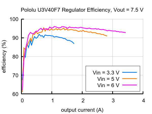
- Typical efficiency of 90% to 95%, depending on input voltage, output voltage, and load (see the efficiency graph below)
- Switching frequency: ~600 kHz under heavy loads
- Power-save mode with ultrasonic operation that increases light load efficiency by reducing switching frequency, but keeps it above the audible range (20 kHz)
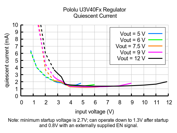
- Typical no-load quiescent currents under 2 mA (see the quiescent current graph below)
- 9.5 A switch allows for:
- Instantaneous input currents up to 9.5 A
- Input currents up to 4.5 A for several seconds
- Input currents up to 4 A for prolonged durations
- Integrated protections:
- Over-temperature shutdown
- Soft-start feature limits inrush current and gradually ramps output voltage
- Output over-voltage protection (typically at 16.5V)
- Cycle-by-cycle input current limiting to 9.5 A while boosting
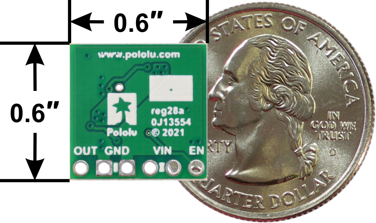
- Compact size: 0.6″ × 0.6″ × 0.22″ (15.2 × 15.2 × 5.6 mm)
- Weight: 1.5 g
Connections
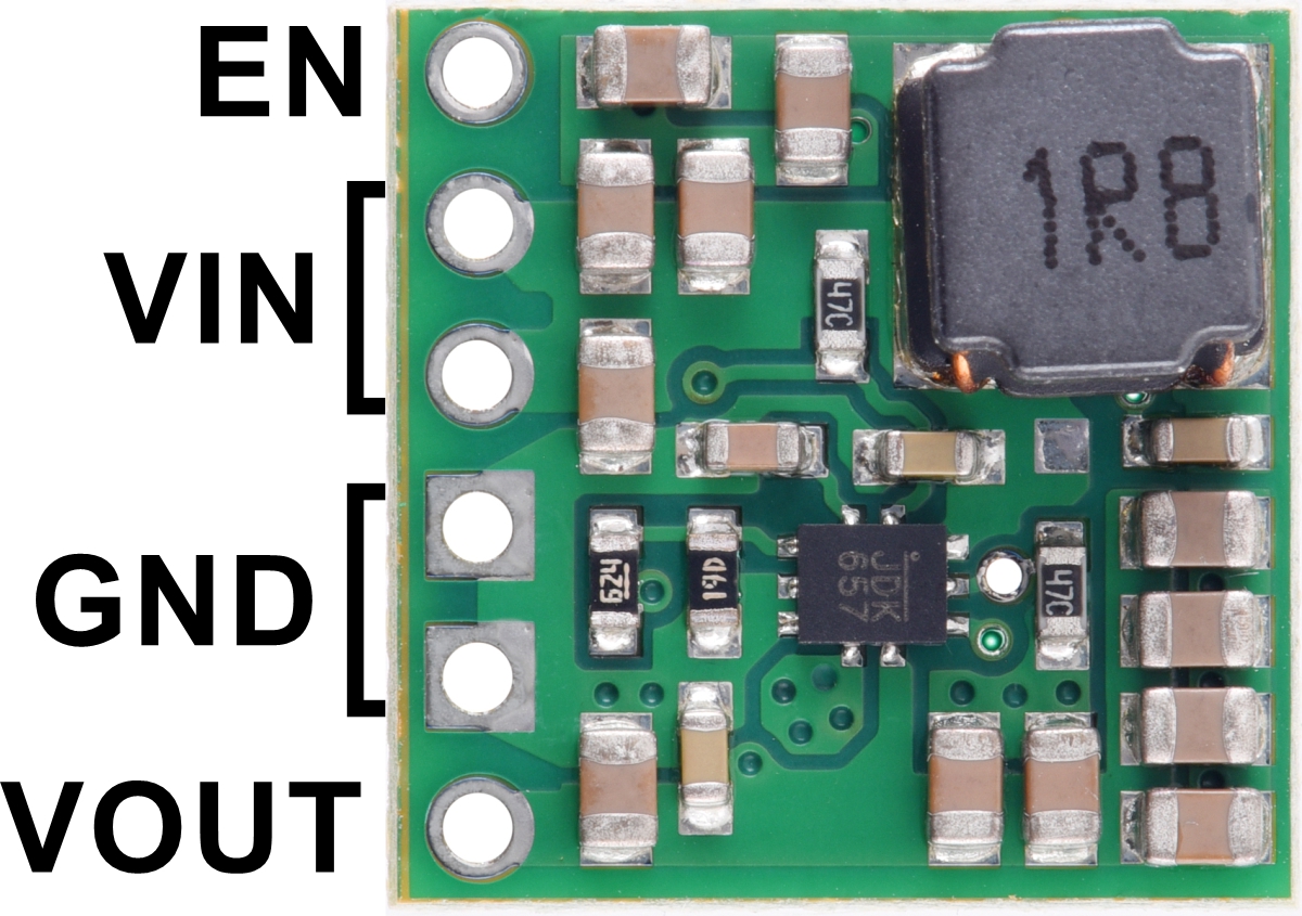 |
The input voltage, VIN, must initially be at least 2.7 V and should not exceed the output voltage, VOUT. (If VIN is higher than VOUT, the higher input voltage will show up on the output, which is potentially dangerous for your connected load and could also damage the regulator.) Once the regulator is on, VIN can fall as low as 0.8 V and the regulator will continue to operate. However, for VIN voltages below 1.3 V, an external source must be used to supply the EN pin (with 1.3 V or more) to keep the regulator enabled.
VOUT is the regulated output voltage. The regulator’s soft-start feature gradually ramps up the VOUT voltage on start-up to limit in-rush current draw. In our testing that allowed it to start into moderately sized capacitive loads (a few hundred µF) without issue. However, the U3V40Fx regulators do not have short-circuit protection so they could be damaged if exposed to output shorts or loads that draw excessive in-rush currents. We do not recommend using them with super capacitors or constant current loads beyond their maximum continuous ratings.
The regulator is enabled by default: a 30 kΩ pull-up resistor on the board connects the EN pin to VIN. The enable pin can be driven low (under 0.4 V) to disable the regulator and put the board into a low-power state. However, please note that due to their standard boost regulator topology, the U3V40Fx family of regulators has no way of disconnecting power from the load, so the input voltage will pass directly through to VOUT when the regulator is disabled. The quiescent current draw is typically under 2 mA with no load (see the quiescent current graph below).
By adding a resistor R between EN and GND, it is possible to set a precise low-VIN cutoff threshold. The following equations show the relationship between the cutoff voltage in volts and R in kΩ:
``R = (text(36.9)) / (V_text(cutoff ) – 1.38)``
Included hardware
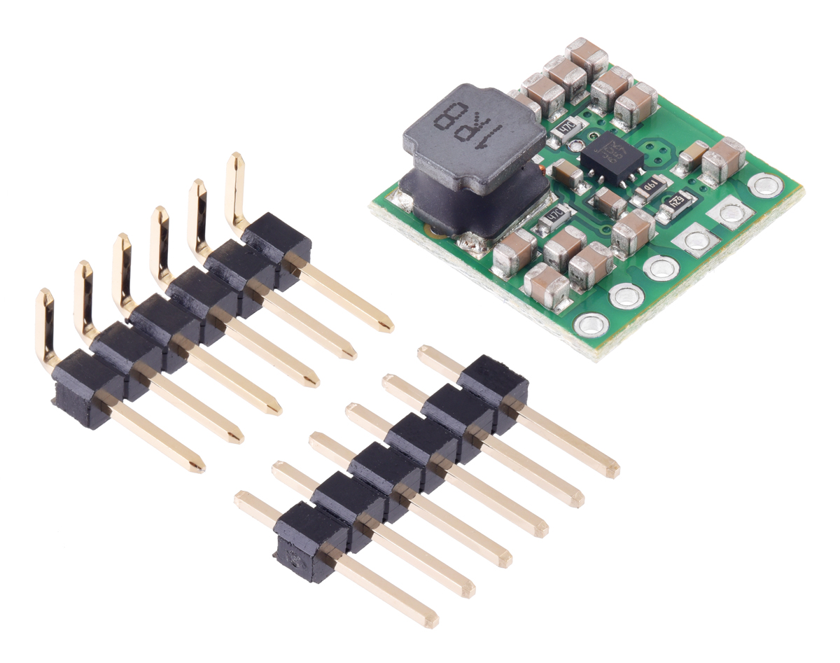 |
Step-Up Voltage Regulator U3V40Fx, with included hardware. |
|---|
The connections are labeled on the back side of the PCB and are arranged with a 0.1″ spacing along the edge of the board for compatibility with solderless breadboards, connectors, and other prototyping arrangements that use a 0.1″ grid. You can solder wires directly to the board or solder in either the 6×1 straight male header strip or the 6×1 right-angle male header strip that is included.
The connections for VIN and GND are duplicated allowing two header pins to be used for each connection. Note that each header pin is only rated for 3 A (6 A combined per pair), and solderless breadboards are usually not intended to handle more than a few amps.
Typical efficiency
The efficiency of a voltage regulator, defined as (Power out)/(Power in), is an important measure of its performance, especially when battery life or heat are concerns. As shown in the graphs below, the U3V40F5 regulator has an efficiency of 90% to 95% for most combinations of input voltage, output voltage, and load.
 |
Maximum continuous output current
The maximum achievable output current is approximately proportional to the ratio of the input voltage to the output voltage. Additionally, the maximum output current can depend on other factors, including the ambient temperature, air flow, and heat sinking. The graph below shows the typical maximum continuous output currents these regulators can deliver at room temperature with no forced airflow or heat sinking.
 |
During normal operation, this product can get hot enough to burn you. Take care when handling this product or other components connected to it.
Quiescent current
The quiescent current is the current the regulator uses just to power itself, and the graph below shows this for the different regulator versions as a function of the input voltage. The module’s EN input can be driven low to put the board into a low-power state where it typically draws about 35 µA per volt on VIN.
 |
LC Voltage Spikes
When connecting voltage to electronic circuits, the initial rush of current can cause damaging voltage spikes that are much higher than the input voltage. In our tests with this family of regulator connected with typical power leads (~30″ test clips), we found that input voltages up to 11 V did not generally cause spikes high enough to damage the regulator itself, but even lower input voltages did cause spikes that could still be problematic for boost regulators operating with the input voltage close to the set output voltage, since input voltages above the set output voltage will propagate to the output and could damage circuits being powered by the regulator. An electrolytic capacitor (33 μF is a good starting point) can be added close to the regulator between VIN and GND to help suppress these spikes.
More information about LC spikes can be found in our application note, Understanding Destructive LC Voltage Spikes.
Related products


Related categories


Home | Forum | Blog | Support | Ordering Information | Lists | Distributors | BIG Order Form | About | Contact
© 2001–2026 Pololu Corporation
