Support » Jrk G2 Motor Controller User’s Guide »
8. Pinout and components
The pinout diagrams below identify the I/O and power pins on each Jrk G2 model.
 |
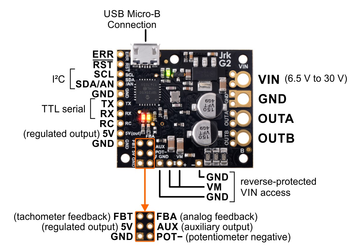
Basic pinout diagram of the Jrk G2 21v3 USB Motor Controller with Feedback. |
|---|
 |
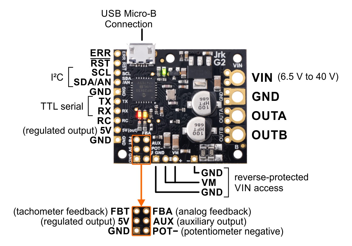
Basic pinout diagram of the Jrk G2 18v19 USB Motor Controller with Feedback. |
|---|
 |
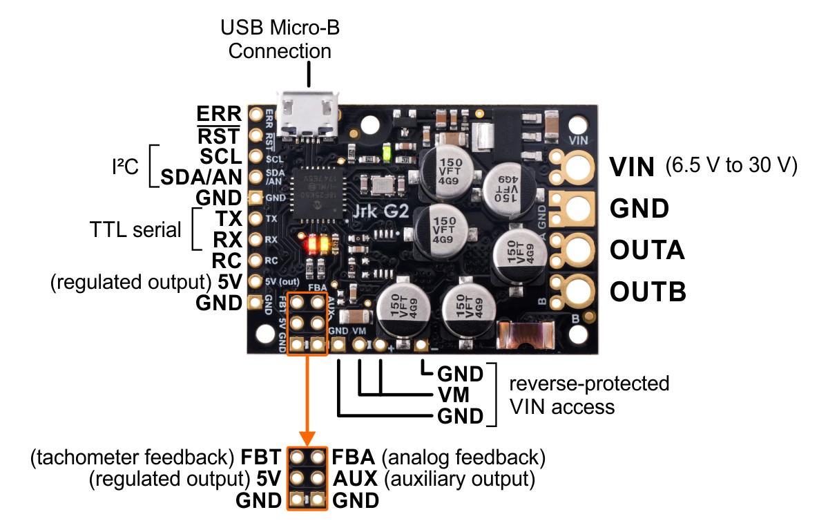
Basic pinout diagram of the Jrk G2 24v13 USB Motor Controller with Feedback. |
|---|
 |
Basic pinout diagram of the Jrk G2 18v27 USB Motor Controller with Feedback. |
|---|
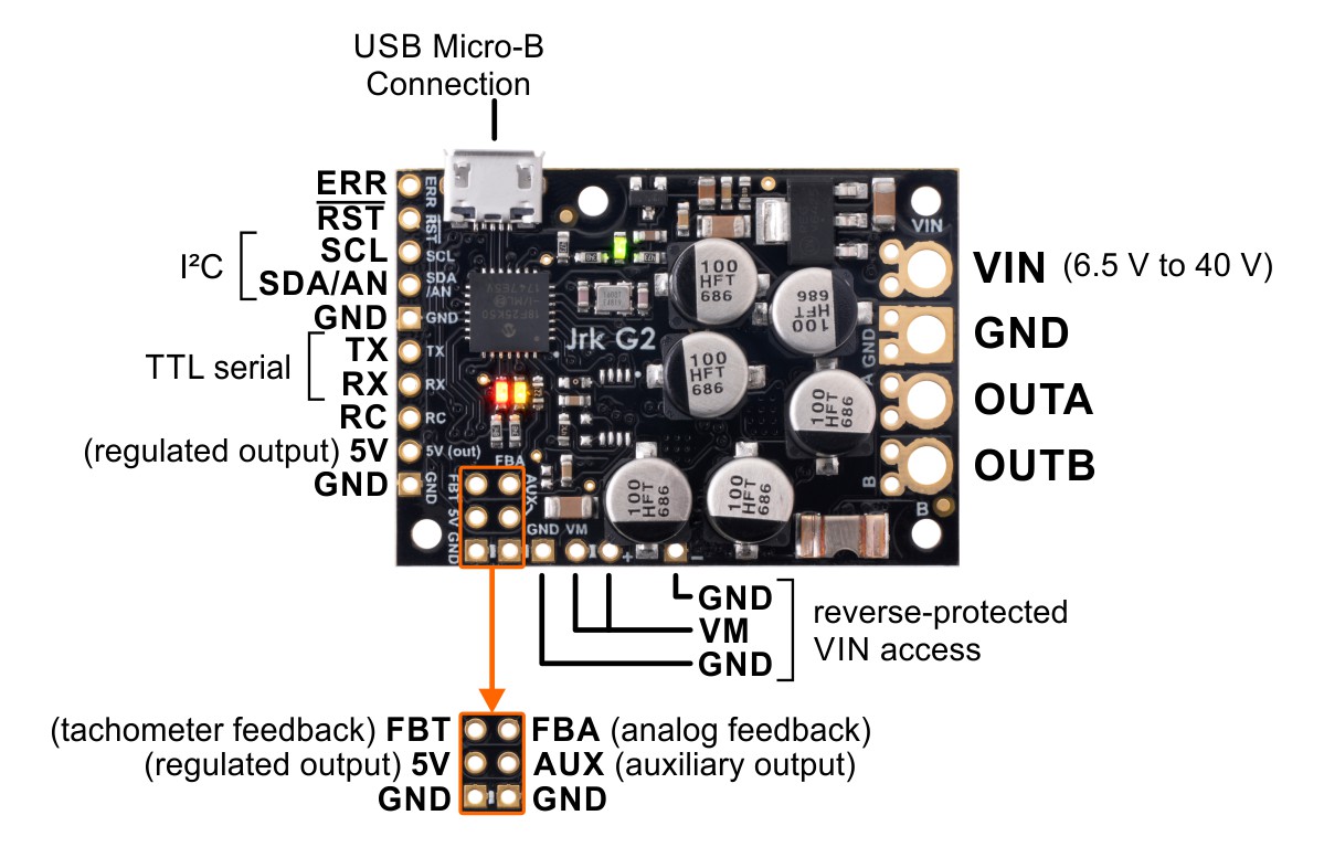 |
Basic pinout diagram of the Jrk G2 24v21 USB Motor Controller with Feedback. |
|---|
The Jrk G2 can connect to a computer’s USB port via a USB A to Micro-B cable (not included). The USB connection is used to configure the Jrk, and it can also be used to send commands, get status information, and send and receive TTL serial bytes.
Power connections
The through-holes on the right side of the board are for motor and power connections: your power supply should be connected to VIN and GND, and your motor leads should be connected to OUTA and OUTB. Section 4.2 goes into detail about connecting a motor and power supply to the Jrk.
A few smaller through-holes along the bottom edge of the board provide access to VM, the reverse-protected motor voltage. On the 24v21 and 18v27 versions, one of these VM access points and the GND access point to its right are partially blocked by a capacitor.
Control pins
The pins in a row along the left side of the PCB are mostly for providing control inputs to the Jrk.
The ERR pin is an optional output that is normally pulled low, but drives high to indicate when an error is stopping the motor. It is tied to the red error LED. For more information about error handling and the ERR pin, see Section 7.7.
The RST pin can be driven low to reset the Jrk’s microcontroller, but this should generally not be necessary for typical applications. The line is pulled up to 5 V so it is safe to leave this pin unconnected. You should wait at least 10 ms after a reset before sending commands to the Jrk.
The SCL and SDA/AN pins provide the Jrk’s I²C interface. For more information about setting up I²C control, see Section 6.3.
Additionally, SDA/AN and SCL serve different functions in analog input mode: SDA/AN is the analog input used to set the target of the system, and SCL can be used to supply 5 V to an input potentiometer and detect if it becomes disconnected. For more information about setting up analog control, see Section 6.4.
The TX and RX pins provide the Jrk’s TTL (0 V to 5 V) serial interface. Serial data can be commands and responses to and from the Jrk, arbitrary data exchanged between the TTL serial interface and the computer via USB, or both. For more information about setting up serial control and using the serial interface, see Section 6.2.
The RC pin is the Jrk’s control input for reading an RC hobby servo signal. For more information about setting up RC control, see Section 6.5.
The 5V pin provides access to the Jrk’s 5 V logic supply. See Section 7.8 for details.
The GND pins provide a ground reference for logic connections. (Note that your power supply ground should be connected to the large GND through-hole on the right side of the board, not the small 0.1″-spaced through-holes on the left.)
Feedback pins
The six grouped pins in the lower left corner of the Jrk PCB allow connection to a feedback sensor.
The FBT pin is the Jrk’s tachometer feedback input, used for a speed-measuring device that generates pulses at a rate proportional to the speed of the output. For information about setting up frequency feedback, see Section 5.3. The 5V and GND pins below FBT provide convenient power and ground connection points for the frequency sensor.
The FBA pin is the Jrk’s analog feedback input, used for a potentiometer or other analog voltage source that indicates the position of the output. For more information about setting up analog feedback, see Section 5.2.
The AUX pin can be used to supply 5 V power to a feedback potentiometer and detect if it becomes disconnected.
The POT− pin can be connected to a feedback potentiometer’s negative terminal and aids with disconnect detection. This pin is not present on the Jrk G2 18v27 and 24v21: those models have a GND pin in the same location that can be used for the same purpose (but does not provide additional disconnect detection like POT−). The POT− pin is connected to GND through an on-board 220Ω resistor.
Hardware design files
These files provide further documentation of the hardware design of the Jrk G2 21v3 motor controller:
- Dimension diagram (215k pdf)
- 3D model (11MB step)
- Drill guide (59k dxf)
These files provide further documentation of the hardware design of the Jrk G2 18v19 and 24v13 motor controllers:
- Dimension diagram (220k pdf)
- 3D model (11MB step)
- Drill guide (83k dxf)
These files provide further documentation of the hardware design of the Jrk G2 18v27 and 24v21 motor controllers:
- Dimension diagram (208k pdf)
- 3D model (11MB step)
- Drill guide (95k dxf)
Related products


Home | Forum | Blog | Support | Ordering Information | Lists | Distributors | BIG Order Form | About | Contact
© 2001–2026 Pololu Corporation
