Electronics » Motion Control Modules » Brushed DC Motor Drivers »
TB9051FTG Single Brushed DC Motor Driver Carrier

This breakout board makes it easy to use Toshiba’s TB9051FTG brushed DC motor driver. It has a wide operating voltage range of 4.5 V to 28 V and can deliver a continuous 2.6 A. A fixed current chopping threshold allows the TB9051 to limit the peak motor current, and it features built-in protection against under-voltage, over-current, and over-temperature conditions; our carrier board also adds reverse-voltage protection.

| Description | Specs (13) | Pictures (9) | Resources (6) | FAQs (0) | On the blog (2) | Distributors (59) |
|---|
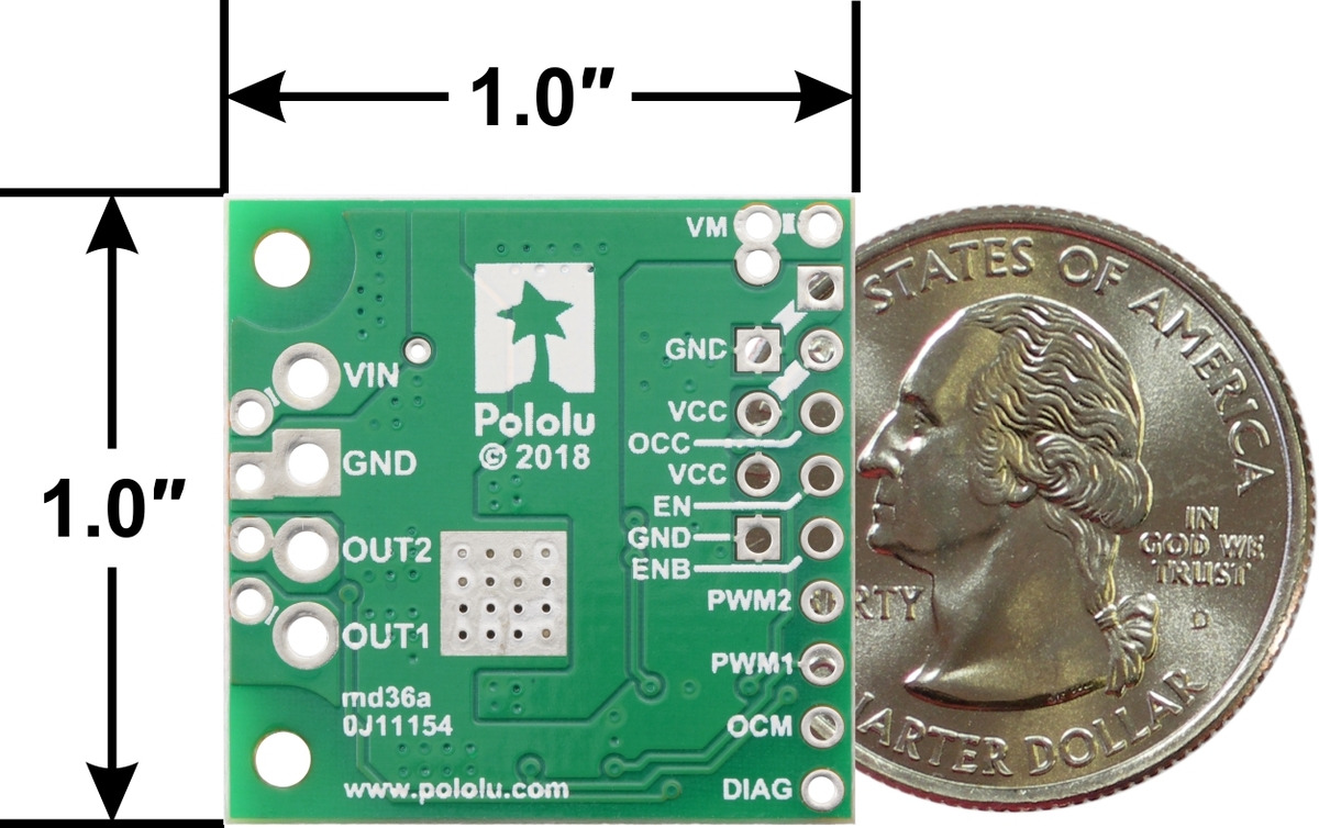 |
TB9051FTG Single Motor Driver Carrier, bottom view with dimensions. |
|---|
Overview
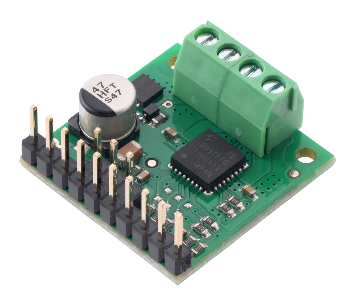
The TB9051FTG from Toshiba is an H-bridge motor driver IC that can be used for bidirectional control of a single brushed DC motor at 4.5 V to 28 V. It can supply up to about 2.6 A continuously, and it can deliver peak currents up to 5 A (typical) for a few seconds. The TB9051FTG is a great IC, but its small surface-mount package makes it difficult for the typical student or hobbyist to use; our breakout board makes it easy to use with standard solderless breadboards and 0.1″ perfboards.
Since this board is a carrier for the TB9051FTG, we recommend careful reading of the TB9051FTG datasheet (2MB pdf). The board ships populated with SMD components, including the TB9051FTG and a reverse battery protection circuit.
For those who need to control two motors, we also have dual-channel TB9051FTG boards available in the form factors of a Raspberry Pi expansion board and an Arduino shield (the shield version is also designed to work as a general-purpose dual motor driver that can be used with other microcontroller boards outside of the Arduino environment).
Features
- Single-channel H-bridge motor driver
- Motor supply voltage: 4.5 V to 28 V
- Output current: up to 2.6 A continuous (5 A peak)
- Automatic current chopping feature helps prevent overheating by gracefully reducing power rather than abruptly shutting down
- Under-voltage lockout and protection against over-current/short-circuit and over-temperature
- Carrier board adds reverse-voltage protection
- Active-low error output indicates over-current, over-temperature, under-voltage, or VCC over-voltage condition
- Compact size (1.0″ × 1.0″)
- Exposed solderable ground pad below the driver IC on the bottom of the PCB
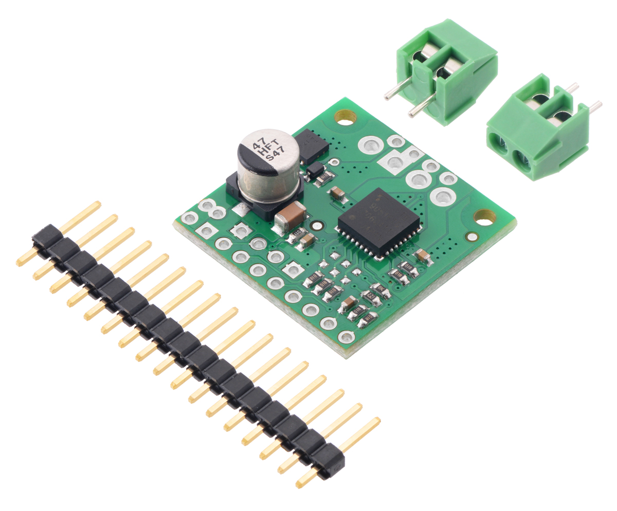
Included hardware
This product ships with all surface-mount components—including the TB9051FTG driver IC—installed as shown in the product picture. However, soldering is required for assembly of the included through-hole parts: one 1×17-pin breakaway 0.1″ male header and two 2-pin, 3.5 mm terminal blocks (for board power and motor outputs).
The 0.1″ male header can be broken or cut into smaller pieces as desired and soldered into the smaller through-holes. These headers are compatible with solderless breadboards, 0.1″ female connectors, and our premium and pre-crimped jumper wires. The terminal blocks can be soldered into the larger holes to allow for convenient temporary connections of unterminated power and motor wires (see our short video on terminal block installation). You can also solder your motor leads and other connections directly to the board for the most compact installation.
|
|
Using the motor driver
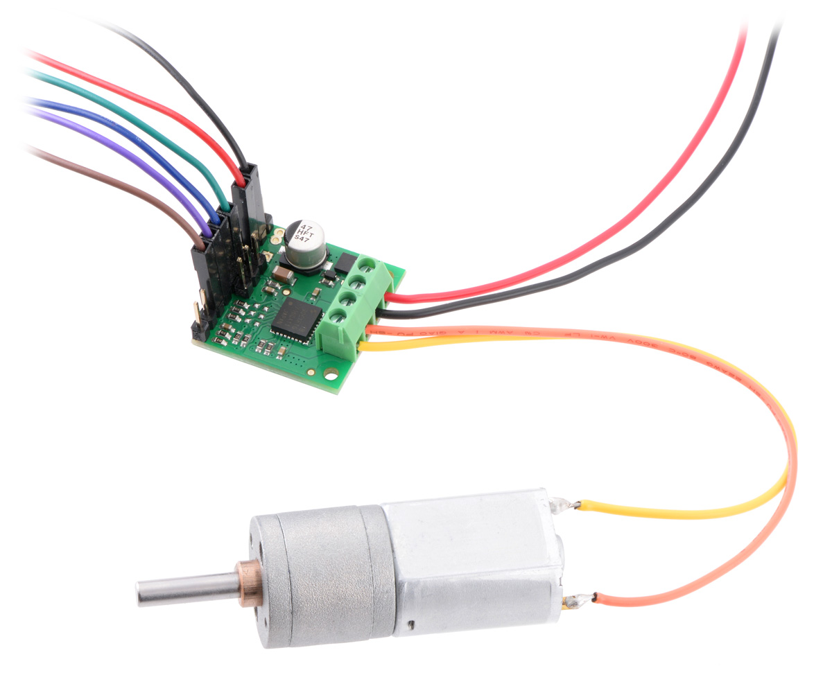 |
Motor and power connections are made on one side of the board and control connections are made on the other. The driver requires an operating voltage between 4.5 V and 28 V to be supplied to the reverse-protected power input, VIN, and a 5 V regulated logic voltage to be supplied to VCC. The VM pin provides convenient access to the reverse-protected motor voltage.
For drive-brake operation (also known as slow decay) with two PWM-capable control lines, the enable pins’ default states can be overridden (EN tied high and ENB tied low) to enable the driver; the adjacent VCC and GND pins provide convenient places to make these connections. The two PWM pins then control the state of the corresponding outputs (up to 20 kHz PWM frequency), as shown in the following simplified truth table:
| TB9051FTG simplified truth table (PWM1 + PWM2) | ||||||
|---|---|---|---|---|---|---|
| Inputs | Outputs | Operation | ||||
| EN | ENB | PWM1 | PWM2 | OUT1 | OUT2 | |
| 1 | 0 | PWM | 0 | PWM (H/L) | L | forward/brake at speed PWM % |
| 0 | PWM | L | PWM (H/L) | reverse/brake at speed PWM % | ||
| 0 | 0 | L | L | brake low (outputs shorted to ground) | ||
| 1 | 1 | L | L | |||
| 0 | X | X | X | Z | Z | coast (outputs floating/disconnected) |
| X | 1 | X | X | Z | Z | |
Alternatively, you can hold PWM1 and PWM2 at fixed levels to set the motor direction and apply a PWM signal to EN (or an inverted PWM signal to ENB) to set the speed, which results in drive-coast operation (also known as fast decay). This increases the number of I/O lines to three, but only one of them needs to be PWM-capable, as shown in this simplified truth table:
| TB9051FTG simplified truth table (PWM1 + PWM2 + EN) | ||||||
|---|---|---|---|---|---|---|
| Inputs | Outputs | Operation | ||||
| EN | ENB | PWM1 | PWM2 | OUT1 | OUT2 | |
| PWM | 0 | 1 | 0 | PWM (H/Z) | PWM (L/Z) | forward/coast at speed PWM % |
| 0 | 1 | PWM (L/Z) | PWM (H/Z) | reverse/coast at speed PWM % | ||
| 0 | X | X | X | Z | Z | coast (outputs floating/disconnected) |
| X | 1 | X | X | Z | Z | |
However, note that this second method restricts the PWM frequencies usable with the driver: the motor outputs on the TB9051FTG have a minimum off-time of about 80 microseconds when turned off with EN or ENB, which limits the maximum achievable duty cycle and makes PWM frequencies above a few kilohertz mostly impractical. For example, at 1.25 kHz, each PWM period has a length of 800 µs; if the outputs are off for at least 80 µs, the maximum achievable duty cycle is 90%.)
The TB9051FTG drives its DIAG pin low whenever an under-voltage, VCC over-voltage, over-temperature, or over-current condition occurs. DIAG will also be low whenever either of the enable pins is disabling the driver (they both disable the driver by default). Otherwise, during normal operation, the board pulls DIAG up to VCC.
Over-temperature errors are latched, so the motor outputs will stay off and the DIAG pin will stay asserted until the fault is cleared by toggling one of the enable pins or disconnecting power to the driver. After an over-current error, the driver’s behavior depends on the state of the OCC pin: if OCC is low (default), the outputs remain disabled until the fault is cleared, but if OCC is high, the driver will automatically try to resume operation after a fixed off-time (typically 500 ms). Regardless of the state of OCC, the DIAG pin remains asserted after an over-current error until the fault is cleared.
Under-voltage and VCC over-voltage errors are not latched (the driver will release the DIAG pin and resume operating as soon as the voltage is corrected). An exception is if the driver detects an abnormal voltage on start-up; in this case, it will continue asserting DIAG until the fault is cleared, although it will still allow normal operation in the meantime if there are no other active fault conditions.
Pinout
 |
Pinout diagram of the TB9051FTG Single Brushed DC Motor Driver Carrier. |
|---|
The default states of some of the TB9051FTG logic input pins requires that external connections be made to use this motor driver. To reduce the number of necessary external connections, the board has three locations where an input can be jumpered to an adjacent pin to override the default. The OCC and EN default-overriding jumpers provide connections to VCC, while the ENB jumper provides a connection to GND. The VCC jumper pads are circles; the ground jumper pad is square.
| PIN | Default State | Description |
|---|---|---|
| VIN | Reverse-protected 4.5 V to 28 V board power supply input. | |
| GND | Ground connection points for the motor and logic supplies. | |
| VM | These pins give access to the motor power supply after the reverse-voltage protection MOSFET (see the board schematic below). They can be used to supply reverse-protected power to other components in the system. VM is generally intended as an output, but it can also be used to supply board power, and some of the VM and GND holes are spaced for the addition of an optional through-hole capacitor. | |
| OUT1 | Motor output 1. | |
| OUT2 | Motor output 2. | |
| VCC | 5 V logic supply input. | |
| OCC | LOW | Over-current response configuration input: by default, the driver remains disabled after an over-current condition, but if OCC is high, it automatically tries to resume driving after a short delay instead. |
| EN | LOW | Enable input: when EN is low, OUT1 and OUT2 are set to high impedance. PWM can be applied to this pin (typically done with ENB low and either PWM1 or PWM2 high). The default is for both enable pins to be disabling the driver. |
| ENB | HIGH | Inverted enable input: when ENB is high, OUT1 and OUT2 are set to high impedance. Inverted PWM can be applied to this pin (typically done with EN high and either PWM1 or PWM2 high). The default is for both enable pins to be disabling the driver. |
| PWM1 | LOW | Control/PWM input for OUT1. |
| PWM2 | LOW | Control/PWM input for OUT2. |
| OCM | Current monitor output: this pin provides an analog current-sense feedback voltage of approximately 500 mV per amp (only active while H-bridge is driving) through an on-board RC filter. | |
| DIAG | HIGH | Diagnostic error output: driven low when certain faults have occurred or when the driver is disabled by the EN or ENB inputs. Otherwise, the board pulls this pin up to VCC. |
Current sensing
The current monitor output, OCM, provides an analog current-sense feedback voltage of approximately 500 mV per A. Note that this output is only active while the H-bridge is driving; it is inactive (low) when the driver is braking or the motor output is high impedance (floating). If the driver is braking, current will continue to circulate through the motor, but the voltage on the OCM pin will not accurately reflect the motor current. Please note that like most motor drivers with integrated current sense, the actual sensitivity can vary significantly from unit to unit, and accuracy can be especially poor at low currents (see the TB9051FTG datasheet (2MB pdf) for more information). Please consider our Hall effect current sensors as options for adding more consistent and accurate current sensing to your system.
Real-world power dissipation considerations
The TB9051FTG will start chopping its output current at a typical threshold of 6.5 A. However, the chip by itself will typically overheat at lower currents. In our tests, we found that the chip was able to deliver 5 A for only a few seconds before the chip’s thermal protection kicked in; a continuous current of about 2.6 A was sustainable for many minutes without triggering thermal current limiting or an over-temperature shutdown. The actual current you can deliver will depend on how well you can keep the motor driver cool. The carrier’s printed circuit board is designed to help with this by drawing heat out of the motor driver chip. PWMing the motor will introduce additional heating proportional to the frequency.
Unlike typical H-Bridges, the TB9051FTG has a feature that allows it to gracefully reduce the maximum current limit when the chip temperature approaches its limit. This means that if you push the chip close to its limit, you will see less power to the motor, but it might allow you to avoid a complete shutdown.
This product can get hot enough to burn you long before the chip overheats. Take care when handling this product and other components connected to it.
Schematic diagram
 |
Schematic diagram of the TB9051FTG Single Brushed DC Motor Driver Carrier. |
|---|
This diagram is also available as a downloadable pdf: TB9051FTG single motor driver carrier schematic (147k pdf)
Related products


Home | Forum | Blog | Support | Ordering Information | Lists | Distributors | BIG Order Form | About | Contact
© 2001–2026 Pololu Corporation
