Voltage Regulators and Power Supplies » Step-Down (Buck) Voltage Regulators » APM81815 Step-Down Voltage Regulator Carriers »
APM81815 Step-Down Voltage Regulator Carrier, 5.35V Out
| Output voltage | Typical max output current1 | Input voltage range2 | Size |
|---|---|---|---|
| 5.35 V | 1.1 A | 5.4 V – 72 V | 0.4″ × 0.75″ |
Note 1: At 48 V in. Actual achievable continuous output current is a function of input voltage and is limited by thermal dissipation. See the output current graphs on the product pages for more information.
Note 2: Minimum input voltage is subject to dropout voltage considerations; see the dropout voltage section of product pages for more information.
Alternatives available with variations in these parameter(s): output voltage Select variant…
 Compare all products in APM81815 Step-Down Voltage Regulator Carriers.
| Description | Specs (11) | Pictures (11) | Resources (5) | FAQs (0) | On the blog (0) | Distributors (3) |
|---|
Overview
 |
 |
We are offering these carrier boards with support from Allegro Microsystems as an easy way to use or evaluate their APM81815 step-down voltage regulators; we therefore recommend referencing the APM81815 datasheet (2MB pdf) for detailed documentation of the regulator IC operation.
The APM81815 is a synchronous buck (step-down) voltage regulator that generates lower voltages from input voltages as high as 72 V (80 V absolute maximum). They are switching regulators (also called switched-mode power supplies (SMPS) or DC-to-DC converters), which makes them much more efficient than linear voltage regulators, especially when the difference between the input and output voltage is large. On our boards at room temperature and with no additional heat sinking or airflow, these regulators can typically support continuous output currents between 0.5 A and 1.5 A, depending on the input voltage and output voltage (see the Maximum continuous output current section below). In general, the available output current decreases as the input voltage increases.
This family includes four versions, one for each output voltage supported by the APM81815:
| Item # | Output voltage | Typical max output current(1) |
Input voltage range(2) | Size |
|---|---|---|---|---|
| #5266 | 3.3 V | 1.1 A | 5 V – 72 V | 0.4″ × 0.75″ |
| #5267 | 5 V | 1.1 A | 5.05 V – 72 V | |
| #5268 | 5.35 V | 1.1 A | 5.4 V – 72 V | |
| #5269 | 12 V | 0.8 A | 12.1 V – 72 V | |
| Note 1: At 48 V in. Actual achievable continuous output current is a function of input voltage and is limited by thermal dissipation. See the output current graphs on the product pages for more information. | ||||
| Note 2: Minimum input voltage is subject to dropout voltage considerations; see the dropout voltage section of product pages for more information. | ||||
 |
The regulators feature short circuit protection and thermal shutdown protection, which helps prevent damage from overheating. The boards do not have built-in protection against reverse voltage, but reverse-voltage protection modules are available for adding that functionality.
We manufacture these boards in-house at our Las Vegas facility, so we can make these regulators with customized components to better meet the needs of your project, such as by customizing the FSET pull-down resistor that controls the switching frequency. If you are interested in customization, please contact us for a quote.
Schematic diagram
 |
Schematic diagram of the APM81815 Step-Down Voltage Regulator Carrier. |
|---|
Details for item #5268
This APM81815 is configured to output a fixed 5.35V.
|
|
|
Features
- Input voltage: 5.4 V to 72 V (80 V absolute max)
- Output voltage: 5.35 V with 2% accuracy
- Typical maximum continuous output current: 0.5 A to 1.5 A (see the maximum continuous output current graph below)
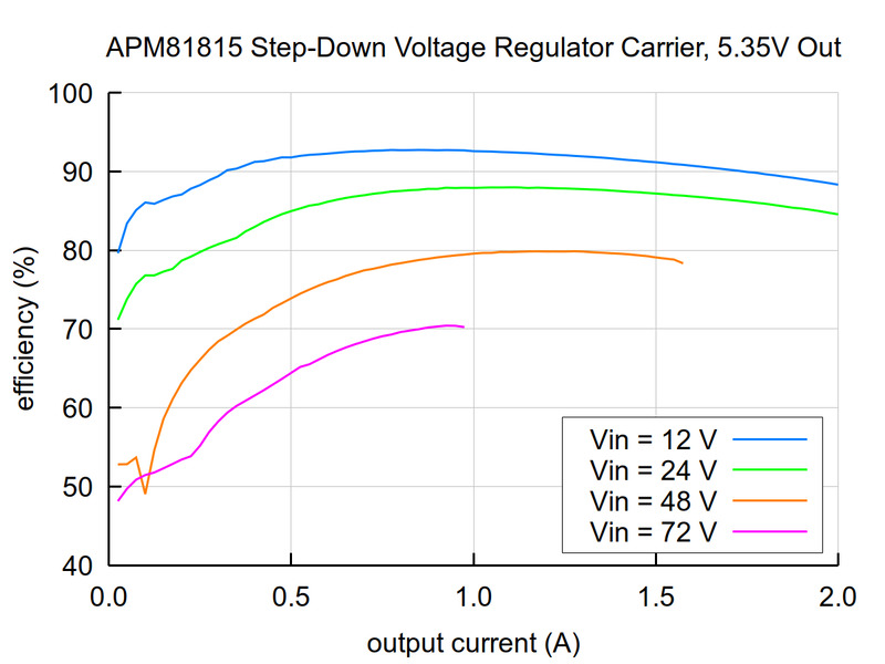
- Typical efficiency of 55% to 95%, depending on input voltage and load (see the efficiency graph below)
- Switching frequency: ~1 MHz under heavy loads
- < 0.1 mA typical no-load quiescent current (see the quiescent current graph below)
- Optional enable input with precision threshold can be used for simple on/off control or to implement a custom low-voltage cutoff
- Soft-start feature limits inrush current and gradually ramps output voltage
- Short-circuit and over-temperature protection
- PCB is 4-layer, 2-oz copper for improved thermal dissipation
- Small size: 0.4″ × 0.75″ × 0.13″ (10.2 mm × 19.1 mm × 3.2 mm)
- Weight: 1.0 g
Connections
 |
This regulator has four connections: enable (EN), input voltage (VIN), ground (GND), and output voltage (VOUT).
The input voltage, VIN, powers the regulator. Voltages between 5 V and 72 V can be applied to VIN, but generally the effective lower limit of VIN is VOUT plus the regulator’s dropout voltage, which varies approximately linearly with the load (see below for graphs of the dropout voltage as a function of the load). Additionally, please be wary of destructive LC spikes (see below for more information).
VOUT is the regulated output voltage.
The regulator, which is enabled by default, can be put into a low-power state that disables the output by reducing the voltage on the EN pin below 1.05 V (typical), and it can be brought out of this state again by increasing the voltage on EN past 1.2 V (typical; the actual rising threshold can vary between 1.15 V and 1.25 V). The shutdown current draw in this sleep mode is dominated by the current through the 100 kΩ pull-up resistor between EN and VIN, resulting in approximately 10-20 μA per volt on VIN. (Note that the shutdown current draw when the regulator is disabled can be greater than the quiescent draw while enabled; see the quiescent current graph below for more details.)
The four connections are labeled on the back side of the PCB and are arranged with a 0.1″ spacing along the edge of the board for compatibility with solderless breadboards, connectors, and other prototyping arrangements that use a 0.1″ grid. You can solder wires or 0.1″ header pins directly to the board. Note: header pins are not included with this product, but 1×4 straight male headers and 1×4 right-angle male headers are available separately.
Typical efficiency
The efficiency of a voltage regulator, defined as (Power out)/(Power in), is an important measure of its performance, especially when battery life or heat are concerns.
 |
Maximum continuous output current
The maximum achievable output current of these regulators varies with the input voltage but also depends on other factors, including the ambient temperature, air flow, and heat sinking. The graph below shows maximum output currents that these APM81815 regulators can deliver continuously on our boards at room temperature in still air and without additional heat sinking.
 |
During normal operation, this product can get hot enough to burn you. Take care when handling this product or other components connected to it.
Quiescent current
The quiescent current is the current the regulator uses just to power itself, and the graph below shows this for the different regulator versions as a function of the input voltage.
 |
Typical dropout voltage
The dropout voltage of a step-down regulator is the minimum amount by which the input voltage must exceed the regulator’s target output voltage in order to ensure the target output can be achieved. For example, if a 5 V regulator has a 1 V dropout voltage, the input must be at least 6 V to ensure the output is the full 5 V. Generally speaking, the dropout voltage increases as the output current increases. (Note that for the 3.3 V version, the dropout is at least 1.7 V due to the regulator’s 5 V minimum operating voltage.) The graphs below shows the dropout voltages for the four different regulator versions as a function of output current.
LC voltage spikes
When connecting voltage to electronic circuits, the initial rush of current can cause voltage spikes that are much higher than the input voltage. If these spikes exceed the regulator’s absolute maximum voltage (80 V), the regulator can be destroyed. In our tests with typical power leads (~30″ test clips), we observed spikes approaching the maximum recommended operating voltage of 72 V at input voltages approaching 40 V. Power supplies or leads with high inductance will make these spikes worse. An electrolytic capacitor (47 μF is a good starting point) can be added close to the regulator between VIN and GND to help suppress these spikes.
More information about LC spikes can be found in our application note, Understanding Destructive LC Voltage Spikes.


