Support » Pololu Dual TB9051FTG Motor Driver Shield User’s Guide » 4. Using as a general-purpose motor driver »
4.b. Board connections
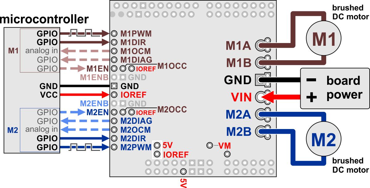 |
Using the dual TB9051FTG motor driver shield with a microcontroller. |
|---|
The above diagram shows the connections typically required to interface this motor driver with a microcontroller.
Pinout
| PIN | Default State | Description |
|---|---|---|
| VIN | Reverse-protected 4.5 V to 28 V board power supply input. | |
| GND | Ground connection points for the motor and logic supplies. The control source and the motor driver must share a common ground. | |
| VM | These pins give access to the motor power supply after the reverse-voltage protection MOSFET (see the board schematic below). They can be used to supply reverse-protected power to other components in the system. VM is generally intended as an output, but it can also be used to supply board power. | |
| 5V | 5 V input. Connected to the TB9051FTG drivers’ VCC pins. | |
| IOREF | Logic supply input. Connect to your microcontroller’s logic voltage. While the TB9051FTG IC does require a 5 V supply to operate, it can accept 3.3 V logic signals. | |
| MxA/B | Output of half-bridge A/B. Each half-bridge connects to one terminal of a DC motor. | |
| MxPWM | LOW | Motor speed inputs: A PWM (pulse-width modulation) signal on these pins corresponds to a PWM output on the corresponding channel’s motor outputs. When a PWM pin is low, the corresponding motor brakes low (both A and B are shorted together through ground). When it is high, the motor is on. The maximum allowed PWM frequency is 20 kHz. |
| MxDIR | LOW | Motor direction inputs: When DIR is high, motor current flows from output A to output B; when DIR is low, current flows from B to A. |
| MxOCM | Current monitor output: this pin provides an analog current-sense feedback voltage of approximately 500 mV per amp (only active while H-bridge is driving) through an on-board RC filter. | |
| MxDIAG | HIGH | Diagnostic error output: driven low when certain faults have occurred or when the driver is disabled by the EN or ENB inputs. Otherwise, the board pulls this pin up to IOREF. |
| MxOCC | LOW | Over-current response configuration input: by default, the driver remains disabled after an over-current condition, but if OCC is high, it automatically tries to resume driving after a short delay instead. |
| MxEN | High | Enable input: when EN is low, OUT1 and OUT2 are set to high impedance. The board pulls this pin up to IOREF. The default is for both enable pins to be enabling the driver. |
| MxENB | LOW | Inverted enable input: when ENB is high, OUT1 and OUT2 are set to high impedance. The board ties this pin to GND. The default is for both enable pins to be enabling the driver. |
Related products


Home | Forum | Blog | Support | Ordering Information | Lists | Distributors | BIG Order Form | About | Contact
© 2001–2026 Pololu Corporation
