

This is a merged information page for Item #4082.
View normal product page.
Pololu item #:
4082
Brand:
Pololu
Status:
Active and Preferred

| Output voltage | Typical max output current* |
Input voltage range | Size | Optional enable input |
Reverse voltage protection |
|---|---|---|---|---|---|
| 5 V | 3 A | 2.8 V – 22 V | 0.9″ × 0.9″ | Up to 20 V |
*For input voltages close to the output. Actual achievable maximum continuous current is a function of input voltage and is limited by thermal dissipation. See the output current graphs on the product page for more information.
Alternatives available with variations in these parameter(s): output voltage Select variant…
Alternatives available with variations in these parameter(s): continuous output current Select variant…
 Compare all products in S13VxFx Step-Up/Step-Down Voltage Regulators.
|
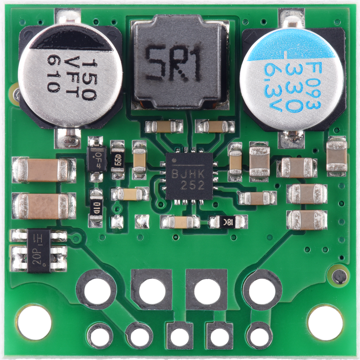
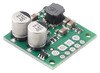
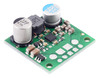
5V Step-Up/Step-Down Voltage Regulator S13V30F5. |
|---|
 |
5V Step-Up/Step-Down Voltage Regulator S13V30F5, top view. |
|---|
 |
5V, 3A Step-Up/Step-Down Voltage Regulator S13V30F5, top view with labeled pinout. |
|---|
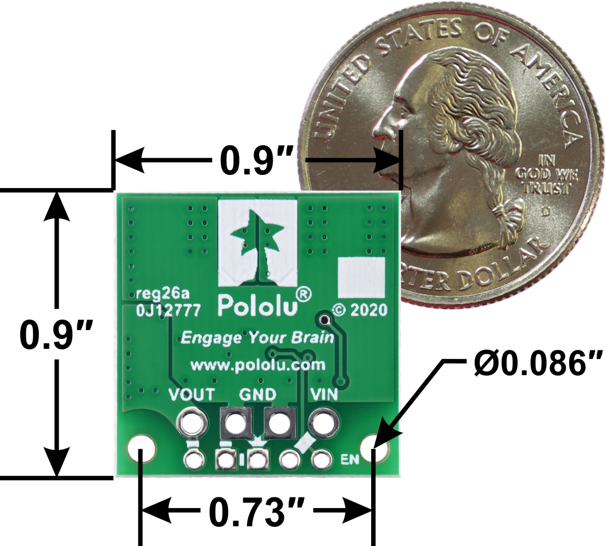 |
5V Step-Up/Step-Down Voltage Regulator S13V30F5, bottom view with dimensions. |
|---|
 |
5V Step-Up/Step-Down Voltage Regulator S13V30F5, with included hardware. |
|---|
 |
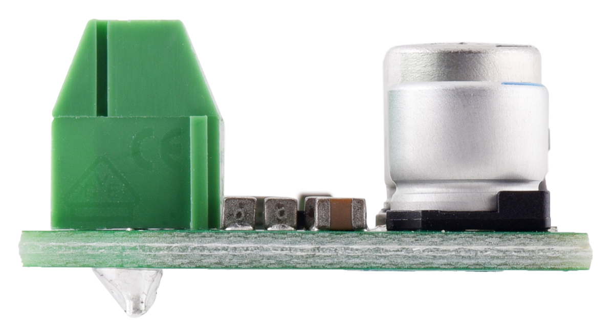
5V Step-Up/Step-Down Voltage Regulator S13V30F5, side view. |
|---|
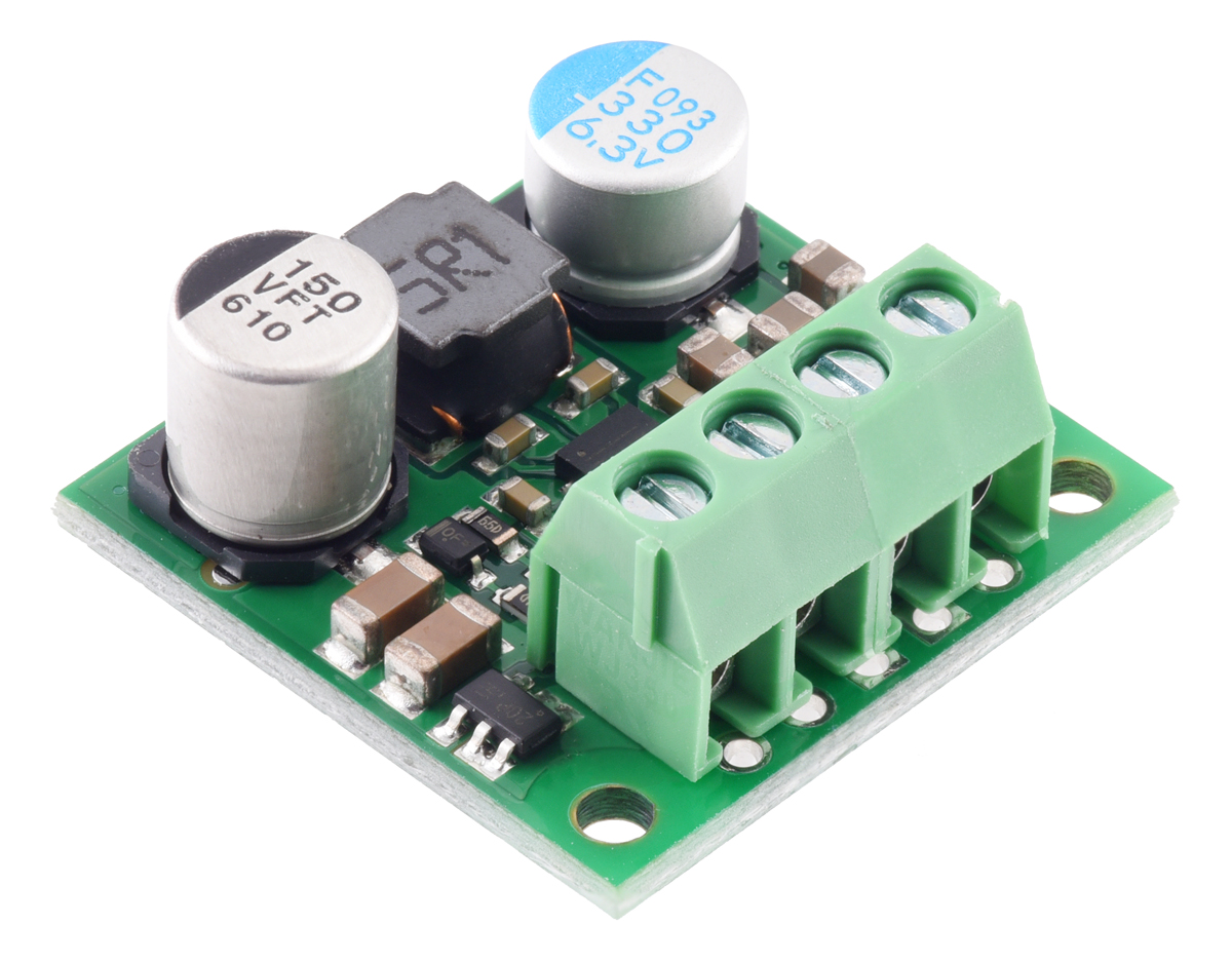 |
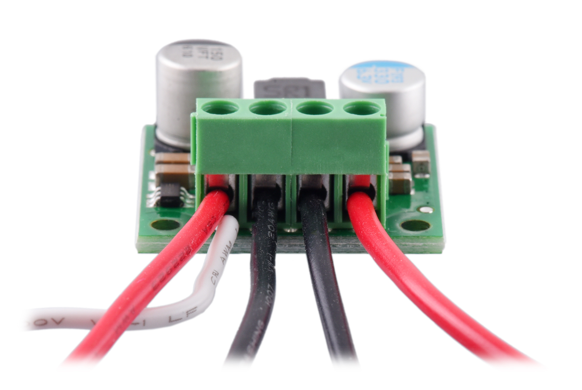
5V Step-Up/Step-Down Voltage Regulator S13V30F5, with terminal blocks installed. |
|---|
 |
5V Step-Up/Step-Down Voltage Regulator S13V30F5, side view with terminal blocks installed |
|---|
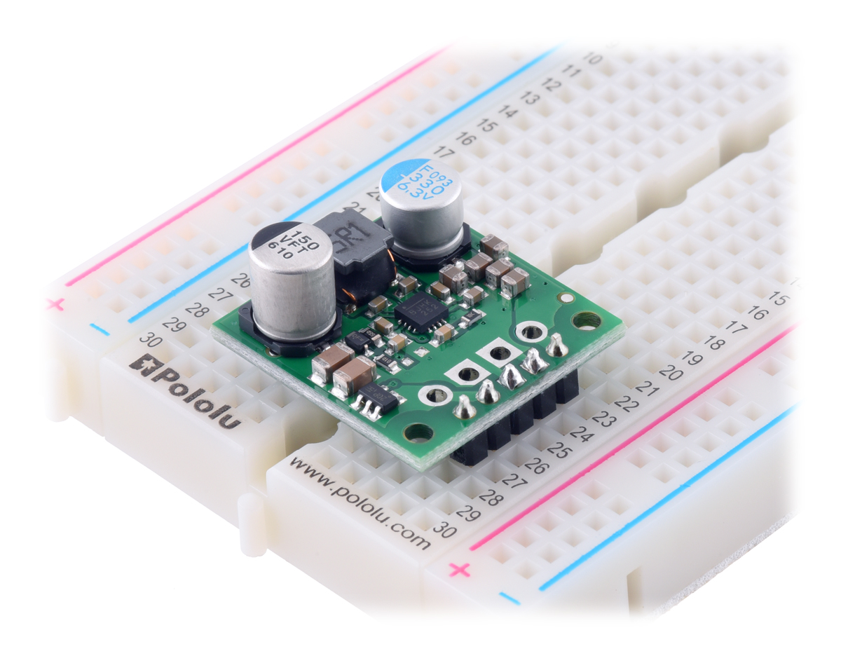 |
5V Step-Up/Step-Down Voltage Regulator S13V30F5, on breadboard. |
|---|
 |
5V Step-Up/Step-Down Voltage Regulator S13V30F5, with terminal blocks and EN wire installed |
|---|
 |
5V Step-Up/Step-Down Voltage Regulator S13V30F5, using all five connections with terminal blocks installed. |
|---|
 |
Typical efficiency of Step-Up/Step-Down Voltage Regulator S13V30F5. |
|---|
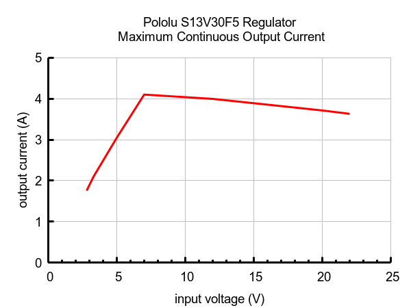 |
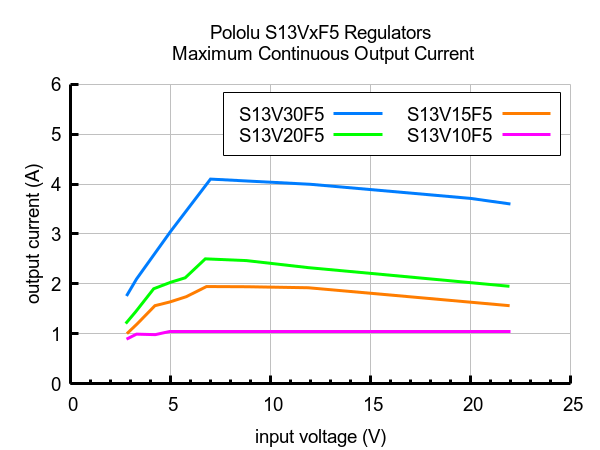
Typical maximum continuous output current of Step-Up/Step-Down Voltage Regulator S13V30F5. |
|---|
 |
Typical quiescent current of Step-Up/Step-Down Voltage Regulator S13V30F5. |
|---|
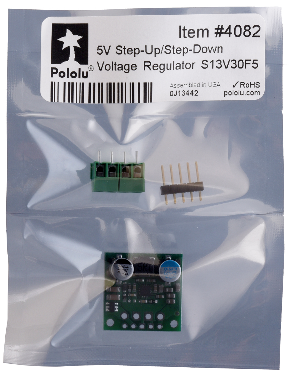 |
Standard packaging for the 5V Step-UpStep-Down Voltage Regulator S13V30F5. |
|---|
|
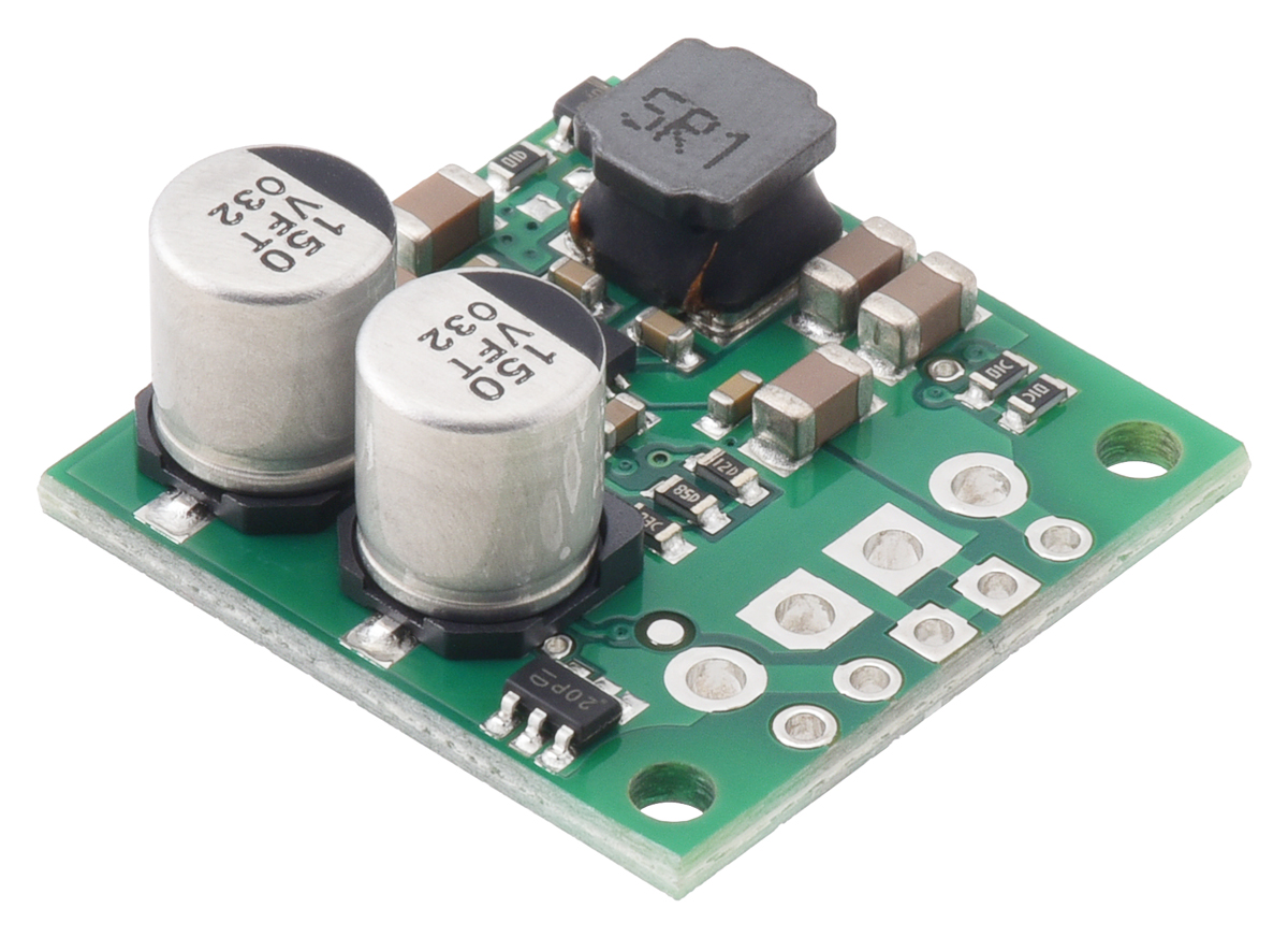
The S13VxF5 family of efficient switching regulators (also called switched-mode power supplies (SMPS) or DC-to-DC converters) use a buck-boost topology to convert both higher and lower input voltages to a regulated 5 V output. They take input voltages from 2.8 V to 22 V and increase or decrease them as necessary, offering a typical efficiency of over 85% and typical continuous output currents between 1 A and 3 A . The flexibility in input voltage offered by this family of regulators is especially well-suited for battery-powered applications in which the battery voltage begins above 5 V and drops below as the battery discharges. Without the typical restriction on the battery voltage staying above the required voltage throughout its life, new battery packs and form factors can be considered.
This product is the larger (0.9″ × 0.9″) S13V30F5, which can output up to around 3 A continuous and has reverse-voltage protection up to 20 V. The other three members of the S13VxF5 family are extra compact (0.35″ × 0.475″) and have lower maximum output currents and no reverse-voltage protection:
The regulators have under-voltage lockout, output over-voltage protection, and over-current protection. A thermal shutdown feature also helps prevent damage from overheating and a soft-start feature limits the inrush current and gradually ramps the output voltage on startup.
 |
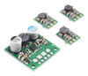
S13VxF5 family of step-up/step-down voltage regulators. |
|---|
 |
3.3V Step-Up/Step-Down Voltage Regulator S13V25F3. |
|---|
The S13V25Fx family, which is pin-compatible with the S13V30F5, consists of six 2.5 A regulators with output voltages ranging from 3.3 V to 15 V:
These versions have the same overall board dimensions as the S13V30F5, but please note that the tall components (i.e. electrolytic capacitors and inductor) are in different locations.
|
5V Step-Up/Step-Down Voltage Regulator S13V30F5. |
|---|
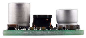 |
5V Step-Up/Step-Down Voltage Regulator S13V30F5, side view. |
|---|
The step-up/step-down regulator has four connections: enable (EN), the input voltage (VIN), ground (GND), and the output voltage (VOUT). The input voltage, VIN, powers the regulator. Voltages between 2.8 V and 22 V can be applied to VIN. VOUT is the regulated output voltage.
The regulator, which is enabled by default, can be put into a low-power sleep state by bringing the EN pin low. The rising threshold for the EN pin is between 1 V and 1.2 V, and the falling threshold is at most 160 mV lower than that (i.e. the falling hysteresis is 160 mV max). This allows a precise low-VIN cutoff to be set, such as with the output of an external voltage divider powered by VIN, which can be useful for battery powered applications where draining the battery below a particular voltage threshold could permanently damage it. The quiescent current draw in sleep mode is dominated by the current in the 475 kΩ pull-up resistor from ENABLE to VIN and in the reverse-voltage protection circuit, which altogether will be between 2 µA and 10 µA per volt on VIN.
|
The regulator has two sets of through-holes: five smaller holes arranged with a 0.1″ spacing along the edge of the board (for compatibility with standard solderless breadboards and perfboards and connectors that use a 0.1″ grid) and four larger holes intended for 3.5 mm-pitch terminal blocks. VIN, GND, and VOUT are available at both the smaller holes and larger holes, but EN is only available on the smaller row of through-holes.
|
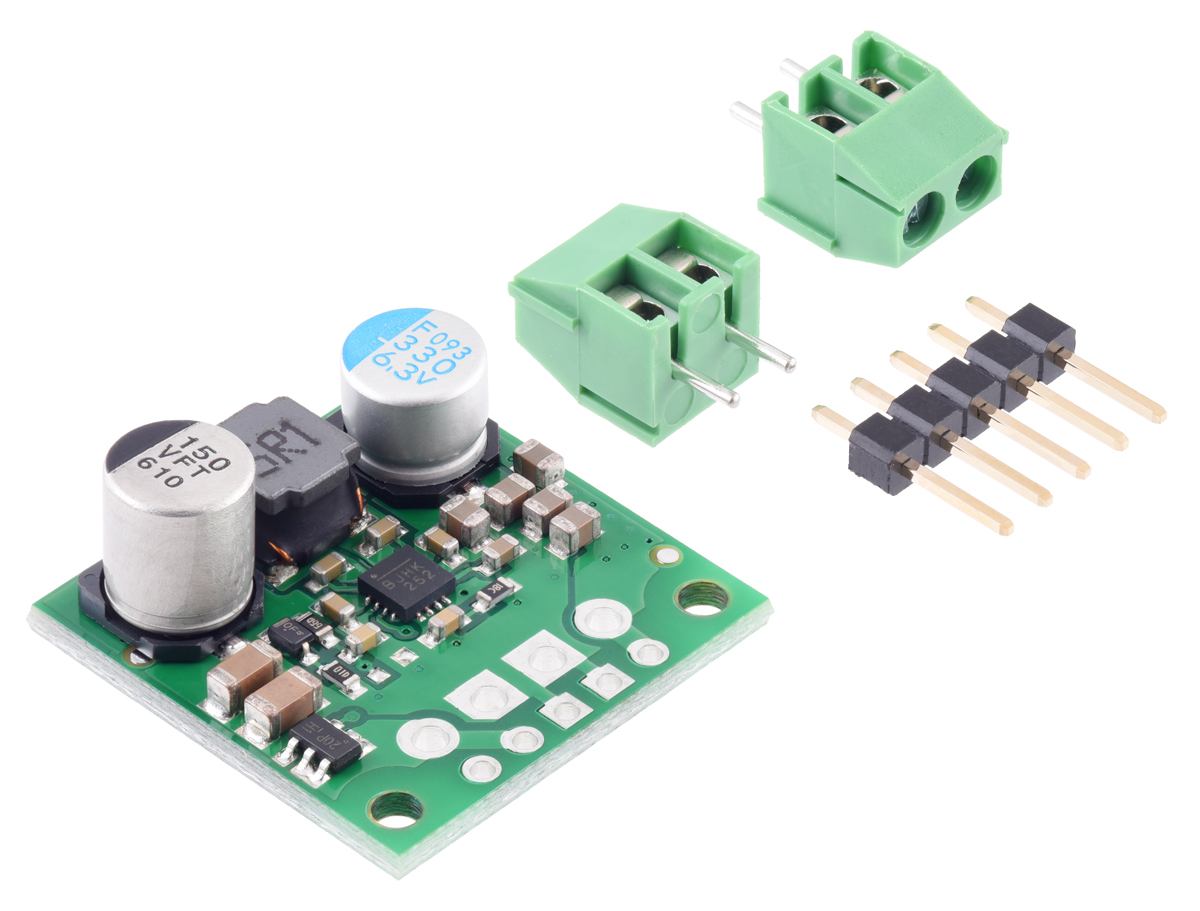
5V Step-Up/Step-Down Voltage Regulator S13V30F5, with included hardware. |
|---|
The regulator includes a 5×1 straight male header strip and two 2-pin, 3.5 mm-pitch terminal blocks, and it can be assembled with either the header or terminal blocks, not both. The 0.1″ male header can be soldered into the smaller through-holes. Alternatively, the terminal blocks can be locked together and soldered into the larger holes to allow for convenient temporary connections of unterminated wires (see our short video on terminal block installation). You can also solder wires directly to the board for the most compact installation.
|
|
If the terminal blocks are used, a small wire (not included) can be soldered to the enable pin as shown below, so it will not interfere with the VIN terminal block connection.
|
|
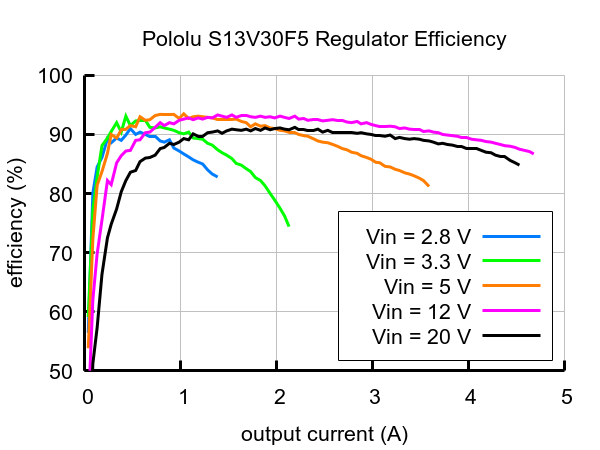
The efficiency of a voltage regulator, defined as (Power out)/(Power in), is an important measure of its performance, especially when battery life or heat are concerns.
 |
The maximum achievable output current of the regulator varies with the input voltage but also depends on other factors, including the ambient temperature, air flow, and heat sinking. The graph below shows maximum output currents that the regulators in the S13VxF5 family can deliver continuously at room temperature in still air and without additional heat sinking.
 |
During normal operation, this product can get hot enough to burn you. Take care when handling this product or other components connected to it.
The quiescent current is the current the regulator uses just to power itself, and the graph below shows this as a function of the input voltage. The module’s EN input can be driven low to put the board into a low-power state where it typically draws between 2 µA and 10 µA per volt on VIN.
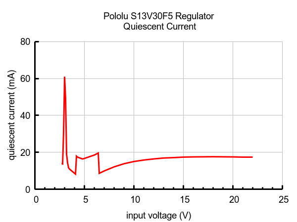 |
Typically the quiescent current of the S13V30F5 is below 20 mA, but for input voltages between about 3 V and 3.3 V the quiescent current of some units can rise to near 100 mA. Keeping connections short and adding a capacitor of a few tens of microfarads greatly reduces this spike in quiescent current.
| Size: | 0.9″ × 0.9″ × 0.38″1 |
|---|---|
| Weight: | 3.5 g2 |
| Minimum operating voltage: | 2.8 V |
|---|---|
| Maximum operating voltage: | 22 V |
| Continuous output current: | 3 A3 |
| Output voltage: | 5 V |
| Reverse voltage protection?: | Y4 |
| Maximum quiescent current: | 100 mA5 |
| Output type: | fixed 5V |
| PCB dev codes: | reg26a |
|---|---|
| Other PCB markings: | 0J12777 |
This DXF drawing shows the locations of all of the board’s holes.
No FAQs available.
We have expanded our S13VxFx family of step-up/step-down voltage regulators to include options with a variety of output voltages from 3.3 V to...
We have released three new members of the S13VxF5 regulator family: 1A Step-Up/Step-Down Voltage Regulator S13V10F5 1.5A Step-Up/Step-Down...
I started routing the PCB for the S13V30F5 5V step-up/step-down voltage regulator in January of 2020, and we were in the middle of testing the...