

This is a merged information page for Item #3786.
View normal product page.
Pololu item #:
3786
Brand:
Pololu
Status:
Active and Preferred

| Output voltage | Typical max output current1 | Input voltage range2 |
|---|---|---|
| 12 V | 2.4 A | 12.9 V – 50 V |
Note 1: At 36 V in. Actual achievable continuous output current is a function of input voltage and is limited by thermal dissipation. See the output current graphs on the product pages for more information.
Note 2: Minimum input voltage is subject to dropout voltage considerations; see the dropout voltage section of product pages for more information.
Alternatives available with variations in these parameter(s): output type Select variant…
 Compare all products in D36V28Fx Step-Down Voltage Regulators.
|
12V, 2.4A Step-Down Voltage Regulator D36V28F12. |
|---|
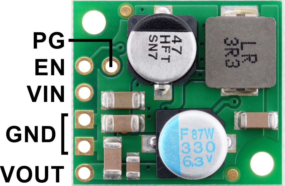 |
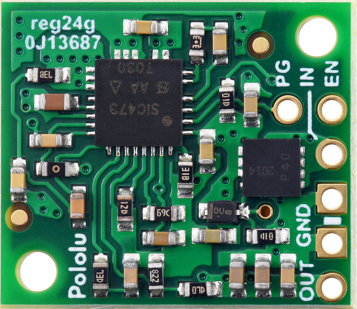
Step-Down Voltage Regulator D36V28Fx, top view with labels. |
|---|
 |
Step-Down Voltage Regulator D36V28Fx, bottom view with dimensions. |
|---|
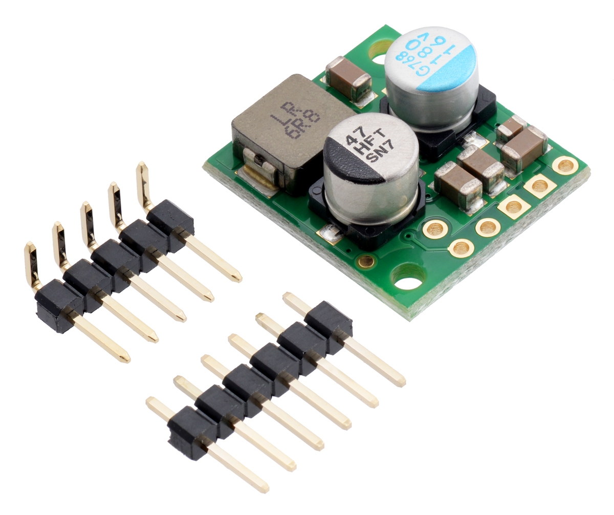 |
Step-Down Voltage Regulator D36V28Fx, with included hardware. |
|---|
 |
12V, 2.4A Step-Down Voltage Regulator D36V28F12, top view. |
|---|
 |
12V, 2.4A Step-Down Voltage Regulator D36V28F12, bottom view. |
|---|
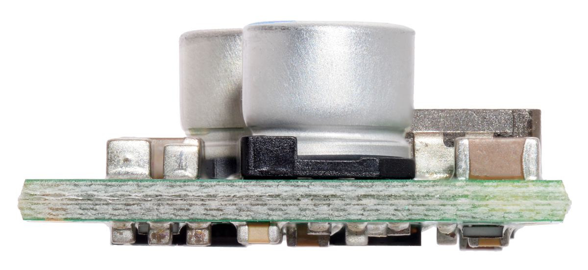 |
Step-Down Voltage Regulator D36V28Fx, side view. |
|---|
 |
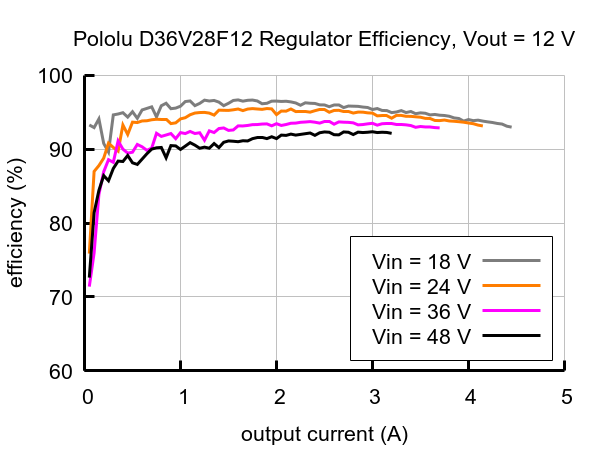
Typical efficiency of Step-Down Voltage Regulator D36V28F12. |
|---|
 |
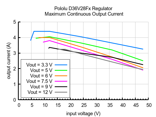
Typical maximum continuous output current of Step-Down Voltage Regulator D36V28Fx. |
|---|
 |
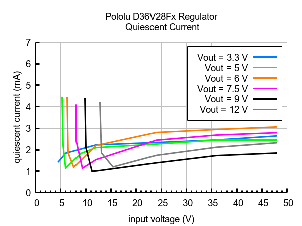
Typical quiescent current of Step-Down Voltage Regulator D36V28Fx. |
|---|
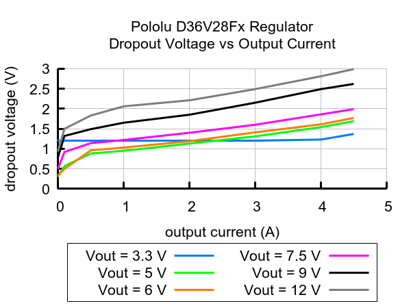 |
Typical dropout voltage of Step-Down Voltage Regulator D36V28Fx. |
|---|
|
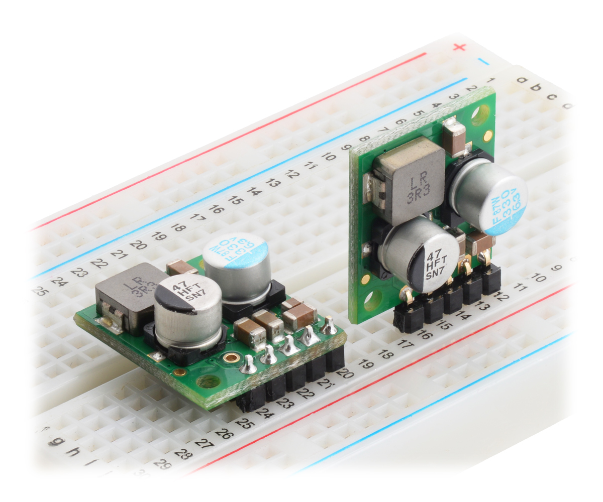 |
Step-Down Voltage Regulator D36V28Fx, assembled on breadboard. |
|---|
The D36V28Fx family of buck (step-down) voltage regulators generates lower output voltages from input voltages as high as 50 V. They are switching regulators (also called switched-mode power supplies (SMPS) or DC-to-DC converters), which makes them much more efficient than linear voltage regulators, especially when the difference between the input and output voltage is large. These regulators can typically support continuous output currents between 2 A and 4 A, depending on the input voltage and output voltage (see the Maximum continuous output current section below). In general, the available output current is a little higher for the lower-voltage versions than it is for the higher-voltage versions, and it decreases as the input voltage increases.
This family includes six versions with fixed output voltages ranging from 3.3 V to 12 V:
The regulators have reverse voltage protection up to 40 V, output undervoltage and overvoltage protection, over-current protection, and short-circuit protection. A thermal shutdown feature also helps prevent damage from overheating and a soft-start feature limits the inrush current and gradually ramps the output voltage on startup.
For lower-voltage applications, consider the very similar D30V30Fx step-down voltage regulators as alternatives. For higher-power applications, consider the D36V50Fx, D42V55Fx, or D42V110Fx families of step-down voltage regulators.
We manufacture these boards in-house at our Las Vegas facility, so we can make these regulators with customized components to better meet the needs of your project, such as by customizing the output voltage. If you are interested in customization, please contact us.
|
|
|
This regulator has six connections: power good (PG), enable (EN), input voltage (VIN), output voltage (VOUT), and two ground (GND) connections.
The “power good” indicator, PG, is an open-drain output that goes low when the regulator’s output voltage either rises more than 20% above or falls more than 10% below the nominal voltage (with hysteresis). An external pull-up resistor is required to use this pin.
The regulator, which is enabled by default, can be put into a low-power sleep state by reducing the voltage on the EN pin below 1.2 V, and it can be brought out of this state again by increasing the voltage on EN past 1.35 V. The quiescent current draw in this sleep mode is dominated by the current in the 100 kΩ pull-up resistor from ENABLE to VIN and in the reverse-voltage protection circuit, which altogether will be between 10 µA and 20 µA per volt on VIN. The tight tolerance of the enable input allows a precise low-VIN cutoff to be set, such as with the output of an external voltage divider powered by VIN, which is useful for battery powered applications where draining the battery below a particular voltage threshold could permanently damage it.
The input voltage, VIN, powers the regulator. Voltages up to 50 V can be applied to VIN. Generally, the effective lower limit of VIN is VOUT plus the regulator’s dropout voltage, which varies approximately linearly with the load (see below for graphs of the dropout voltage as a function of the load).
VOUT is the regulated output voltage.
|
Step-Down Voltage Regulator D36V28Fx, with included hardware. |
|---|
The six connections are arranged on a 0.1″ grid for compatibility with solderless breadboards, connectors, and other prototyping arrangements that use a 0.1″ grid. The PG connection is the only one not located along the edge of the board. A 6×1 straight male header strip and a 5×1 right-angle male header strip are included with the regulator; one pin of the straight header can optionally be broken off and soldered into PG.
 |
Step-Down Voltage Regulator D36V28Fx, side view. |
|---|
The efficiency of a voltage regulator, defined as (Power out)/(Power in), is an important measure of its performance, especially when battery life or heat are concerns.
 |
The maximum achievable output current of these regulators varies with the input voltage but also depends on other factors, including the ambient temperature, air flow, and heat sinking. The graph below shows maximum output currents that these regulators can deliver continuously at room temperature in still air and without additional heat sinking.
 |
During normal operation, this product can get hot enough to burn you. Take care when handling this product or other components connected to it.
The quiescent current is the current the regulator uses just to power itself, and the graph below shows this for the different regulator versions as a function of the input voltage. The module’s EN input can be driven low to put the board into a low-power state where it typically draws between 10 µA and 20 µA per volt on VIN.
 |
The dropout voltage of a step-down regulator is the minimum amount by which the input voltage must exceed the regulator’s target output voltage in order to ensure the target output can be achieved. For example, if a 5 V regulator has a 1 V dropout voltage, the input must be at least 6 V to ensure the output is the full 5 V. Generally speaking, the dropout voltage increases as the output current increases. The graph below shows the dropout voltages for the different members of this regulator family:
 |
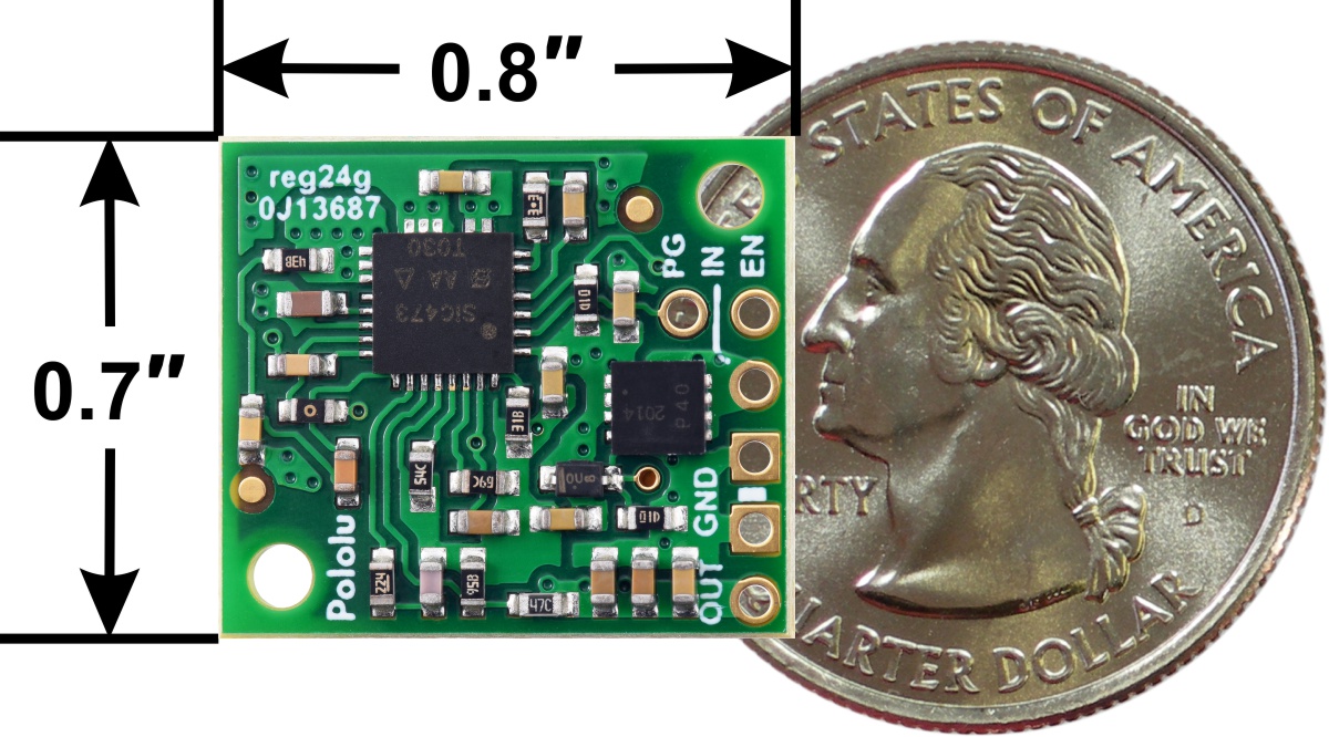
| Size: | 0.7″ × 0.8″ × 0.345″1 |
|---|---|
| Weight: | 3.3 g1 |
| Minimum operating voltage: | 12.9 V2 |
|---|---|
| Maximum operating voltage: | 50 V |
| Continuous output current: | 2.4 A3 |
| Output voltage: | 12 V |
| Reverse voltage protection?: | Y4 |
| Maximum quiescent current: | 3 mA5 |
| Output type: | fixed 12V |
| PCB dev codes: | reg24a, reg24g |
|---|---|
| Other PCB markings: | 0J11946, 0J13687 |
This DXF drawing shows the locations of all of the board’s holes.
No FAQs available.
I am happy to announce the release of our newest regulators, the D36V28Fx family of step-down voltage regulators. These regulators support a wide...