This is a merged information page for Item #2870.
View normal product page.
Pololu item #:
2870
Brand:
Pololu
Status:
Active and Preferred

| Output voltage | Typical max output current1 | Input voltage range | Low-voltage cutoff | Size |
|---|---|---|---|---|
| 5 V (6 V selectable) | 1.7 A | 2 V – 16 V (3 V startup) |
fine-adjust | 0.5″ × 0.60″ × 0.25″ |
Note 1: For input voltages close to the output, after startup. Startup current is limited to approximately 700 mA until output voltage reaches the nominal voltage. After startup, the actual achievable maximum continuous current is a function of input and output voltage and is limited by thermal dissipation. See the output current graphs on the product page for more information.
Alternatives available with variations in these parameter(s): output type low-voltage cutoff Select variant…
 Compare all products in S9V11x Step-Up/Step-Down Voltage Regulators.
|
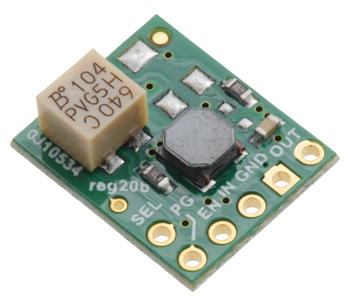
5V Step-Up/Step-Down Voltage Regulator w/ Adjustable Low-Voltage Cutoff S9V11F5S6CMA (silkscreen side). |
|---|
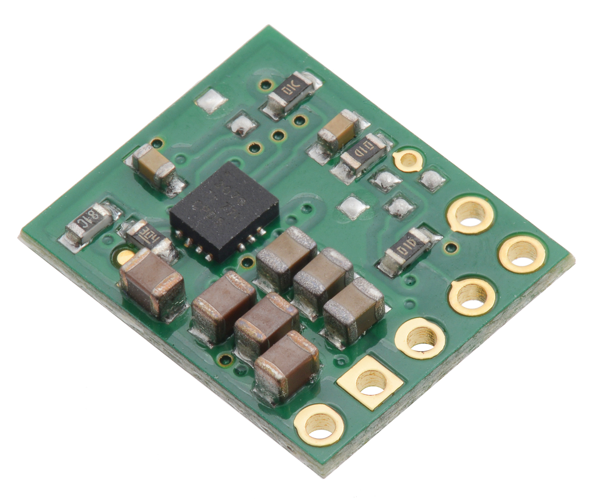 |
5V Step-Up/Step-Down Voltage Regulator w/ Adjustable Low-Voltage Cutoff S9V11F5S6CMA (non-silkscreen side). |
|---|
 |
5V Step-Up/Step-Down Voltage Regulator w/ Adjustable Low-Voltage Cutoff S9V11F5S6CMA with included optional header pins. |
|---|
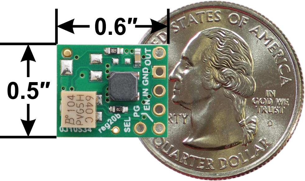 |
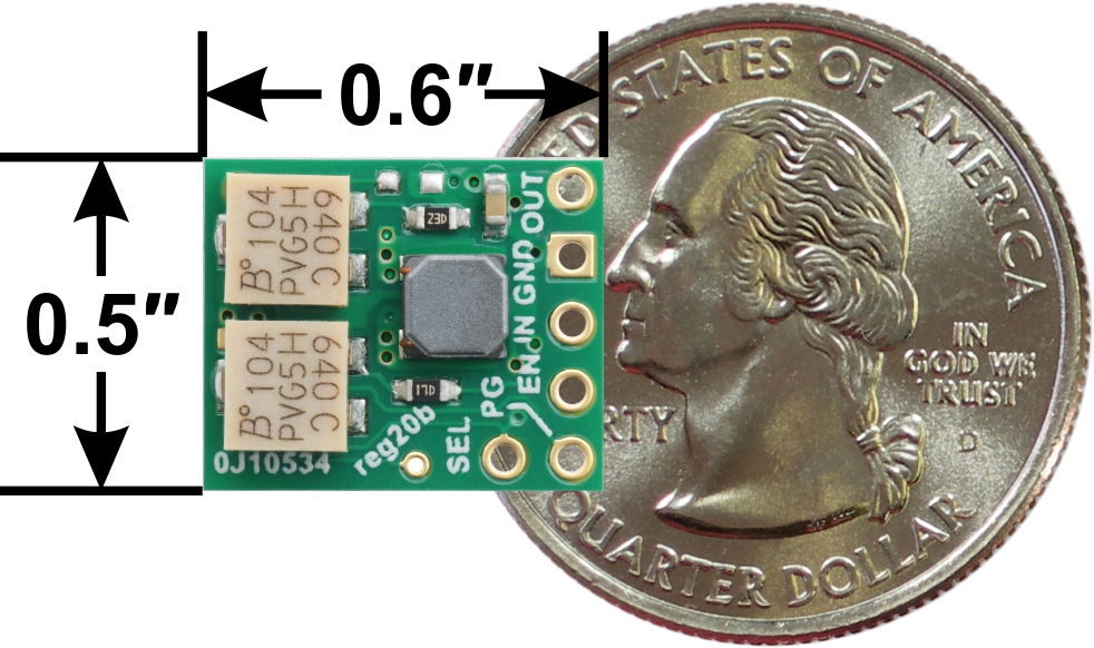
5V Step-Up/Step-Down Voltage Regulator w/ Adjustable Low-Voltage Cutoff S9V11F5S6CMA next to US quarter dollar for size reference. |
|---|
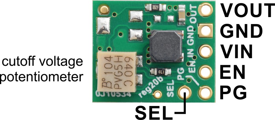 |
5V Step-Up/Step-Down Voltage Regulator w/ Adjustable Low-Voltage Cutoff S9V11F5S6CMA labeled pinout. |
|---|
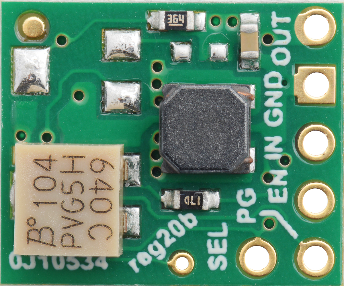 |
5V Step-Up/Step-Down Voltage Regulator w/ Adjustable Low-Voltage Cutoff S9V11F5S6CMA (silkscreen side). |
|---|
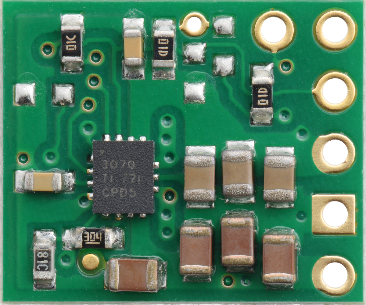 |
5V Step-Up/Step-Down Voltage Regulator w/ Adjustable Low-Voltage Cutoff S9V11F5S6CMA (non-silkscreen side). |
|---|
 |
A multi-turn potentiometer can be used to adjust the low-voltage cutoff of the S9V11xCMA voltage regulators. |
|---|
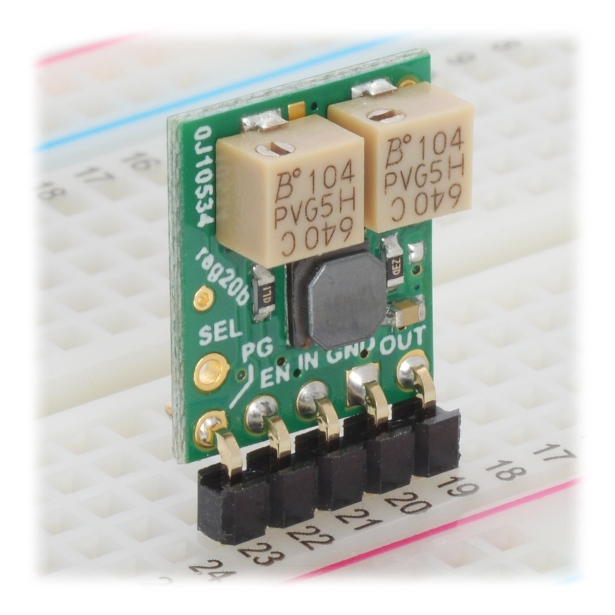 |
Step up/step down regulator S9V11MACMA on a breadboard. |
|---|
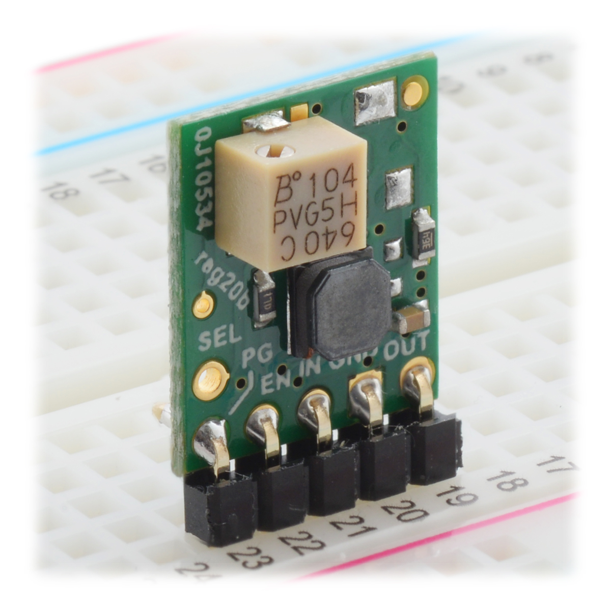 |
Step up/step down regulator S9V11F5S6CMA on a breadboard. |
|---|
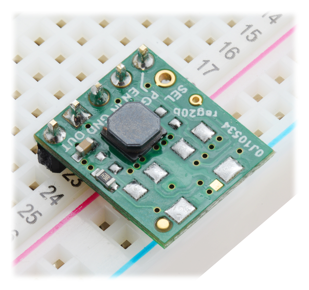 |
Step up/step down regulator S9V11F3S5 on a breadboard. |
|---|
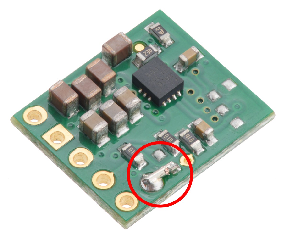 |
To permanently select the alternate output voltage on the S9V11FxSx versions, you can solder a piece of wire between SEL and the unpopulated pad next to it. |
|---|
 |
Typical maximum continuous output current of Step-Up/Step-Down Voltage Regulator S9V11x. |
|---|
 |
Typical efficiency of Step-Up/Step-Down Voltage Regulator S9V11x with VOUT set to 5V. |
|---|
 |
Typical efficiency of Step-Up/Step-Down Voltage Regulator S9V11x with VOUT set to 6V. |
|---|
 |
The S9V11x family of efficient switching regulators (also called switched-mode power supplies (SMPS) or DC-to-DC converters) use a buck-boost topology to convert both higher and lower input voltages to a regulated output voltage. They take input voltages from 2 V to 16 V and increase or decrease them as necessary, offering typical efficiencies of 85% to 95% and typical continuous output currents over 1.5 A for input voltages close to or greater than the output voltage. (Note: The minimum start-up voltage is 3 V, but the regulator will operate down to 2 V after startup.)
The flexibility in input voltage offered by this family of regulators is especially well-suited for battery-powered applications in which the battery voltage begins above the regulated voltage and drops below as the battery discharges. Without the typical restriction on the battery voltage staying above the required voltage throughout its life, new battery packs and form factors can be considered.
These regulators have short-circuit protection, and thermal shutdown prevents damage from overheating. The boards do not have built-in protection against reverse voltage, but reverse-voltage protection modules are available for adding that functionality. Note that the startup current is limited to approximately 700 mA until the output voltage reaches the nominal voltage; after startup, the available current is a function of the input voltage (see the maximum continuous output current graph below).
The different members of this family offer different output voltage options, from fixed voltages (some with selectable alternatives) to adjustable voltages that can be set anywhere between 2.5 V and 9 V. Some versions also have an adjustable low-voltage cutoff that can be set anywhere in the 2 V to 16 V output voltage range and used to prevent your battery from over-discharging. This is particularly useful for battery chemistries that can be damaged when over-discharged, including Li-ion and LiPo. The chart below lists all the regulators in the S9V11x family along with the key features of each version:
| Regulator | Output voltage | Max continuous output current* |
Low-voltage cutoff |
Input voltage range |
Size | Price | |
|---|---|---|---|---|---|---|---|
 |
#5712 S9V11E2F3 | 3.3 V | 1.5 A | – | 2 V – 16 V (3 V startup) |
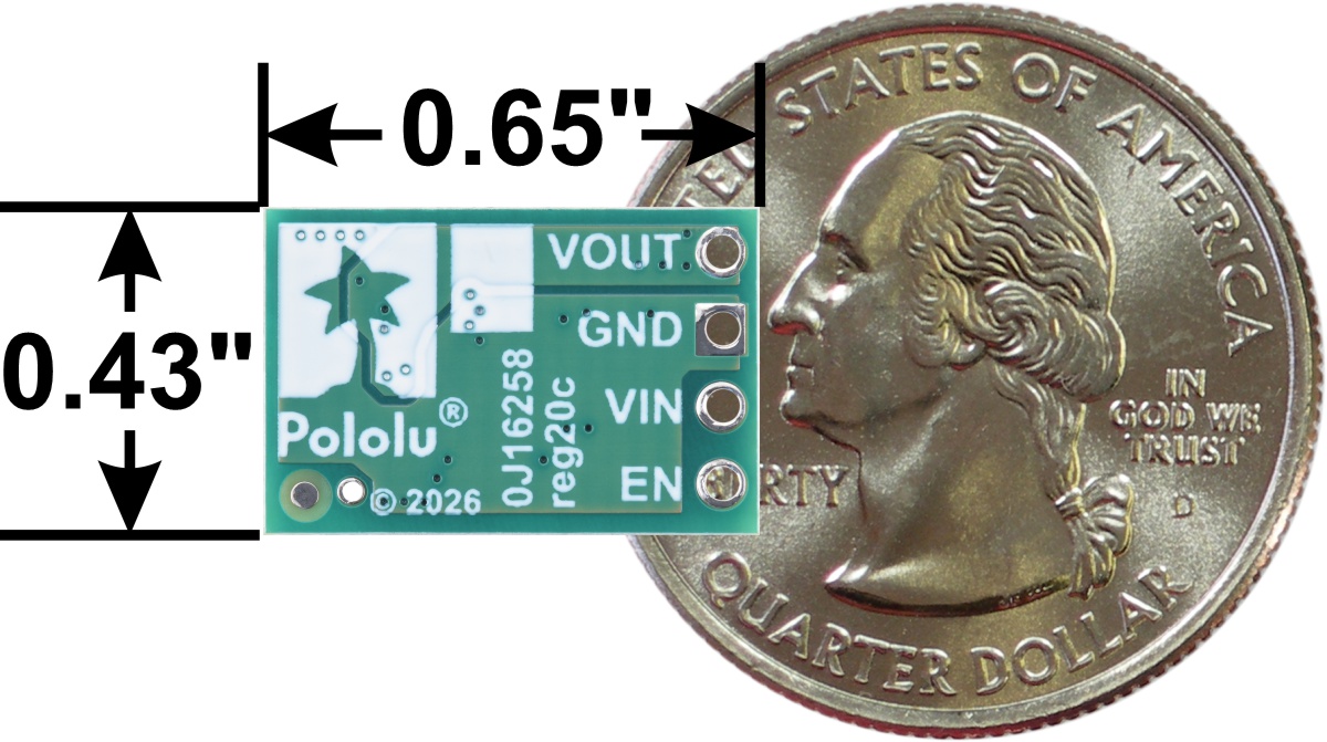
0.43″ × 0.65″ × 0.16″ |
$4.95 |
| #5713 S9V11E2F5 | 5 V | 1.7 A | $4.95 | ||||
| #5714 S9V11E2F6 | 6 V | 1.7 A | $4.95 | ||||
| #5715 S9V11E2F7 | 7.5 V | 1.7 A | $4.95 | ||||
| #5716 S9V11E2F9 | 9 V | 1.7 A | $4.95 | ||||
| #5719 S9V11E2A | 2.5 V – 9 V (adjustable) | 1.7 A | $5.49 | ||||
 |
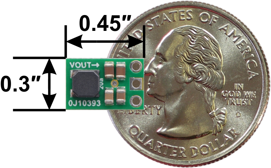
#2836 S9V11F5 | 5 V | 1.5 A | 0.30″ × 0.45″ × 0.17″ |
$6.95 | ||
 |
#2872 S9V11F3S5 | 3.3 V (5 V selectable) | 1.5 A | 0.50″ × 0.60″ × 0.17″ |
$5.95 | ||
| #2873 S9V11F3S5C3 | 3.3 V (5 V selectable) | 1.5 A | 3 V (fixed) | $5.95 | |||
 |
#2869 S9V11MA | 2.5 V – 9 V (precison- adjustable 11-turn pot) |
1.7 A | – | 0.50″ × 0.60″ × 0.25″ |
$9.95 | |
 |
#2870 S9V11F5S6CMA | 5 V (6 V selectable) | 1.7 A | adjustable | $9.95 | ||
| #2871 S9V11F3S5CMA | 3.3 V (5 V selectable) | 1.5 A | adjustable | $9.95 | |||
 |
#2868 S9V11MACMA | 2.5 V – 9 V (precison- adjustable 11-turn pot) |
1.7 A | adjustable | $13.95 | ||
| *For input voltages close to the output, after startup. Startup current is limited to approximately 700 mA until output voltage reaches the nominal voltage. After startup, the actual achievable maximum continuous current is a function of input and output voltage and is limited by thermal dissipation. See the output current graphs on the product pages for more information. | |||||||
|
|
|
We manufacture these boards in-house at our Las Vegas facility, so we can make these regulators with customized components to better meet the needs of your project If you are interested in customization, please contact us for a quote.
This item is the S9V11F5S6CMA, which outputs a fixed 5 V that can be changed to 6 V using a selection input and features a precision-adjustable low-voltage cutoff.
|
|
|
|
The step-up/step-down regulator has five main connections all located along the same edge of the board: the output voltage (VOUT), ground (GND), the input voltage (VIN), an enable input (EN), and a power good indicator (PG). A sixth pin, SEL, can optionally be used to change the output voltage from 5 V to 6 V.
|
The output voltage, VOUT, defaults to 5 V but can be changed to 6 V with output voltage selection pin whose operation is described below.
The input voltage, VIN, should be between 3 V and 16 V when the regulator is first powered. After it is running, it can continue operating down to 2 V. Lower inputs can shut down the voltage regulator; higher inputs can destroy the regulator, so you should ensure that noise on your input is not excessive, and you should be wary of destructive LC spikes (see below for more information).
The regulator features an enable pin, EN, that can be used as a precision low-voltage cutoff thanks to its tight activation and deactivation thresholds (voltages below 0.7 V trigger a low-power sleep state, and voltages above 0.8 V re-enable the regulator). On this regulator version, EN is connected to VIN through a 11-turn potentiometer to provide a user-adjustable cutoff threshold, which is useful for battery powered applications where draining the battery below a particular voltage threshold could permanently damage it. The quiescent current draw in this sleep mode is dominated by the current in the resistor network from ENABLE to VIN, which is approximately 7 µA per volt on VIN (e.g. approximately 20 µA with 3 V in). See the Setting the cutoff voltage section below for details on how to use the built-in potentiometer to set the cutoff threshold.
The “power good” indicator, PG, is an open-drain output that goes low when the regulator’s output falls below around 90% of the nominal voltage, including when the enable pin is held low. The power good indicator is held low until the output reaches 95% of the nominal voltage when it is powering up or coming out of low-power mode. Otherwise, the PG pin is high-impedance, so an external pull-up resistor is required to use this pin.
The select input, SEL, can be driven above 1.1 V (up to 16 V) to change the output voltage of the regulator to 6 V. Driving the pin low or leaving it disconnected sets the output to 5 V. To permanently set the output to 6 V, you can solder a piece of wire between SEL and the unpopulated pad next to it, which is pulled up to VIN; the following picture shows an example of this:
|
The five main through-holes are arranged with a 0.1″ spacing along the edge of the board for compatibility with standard solderless breadboards and perfboards and connectors that use a 0.1″ grid. You can solder wires directly to the board or solder in pieces of the included breakaway 6×1 straight male header strip or the 5×1 right-angle male header strip as desired. The additional straight male header pin can be soldered into the SEL input, though this could prevent the regulator from being used in a breadboard.
|
|
|
|
The low VIN cutoff voltage of the regulator is controlled by adjusting the voltage at the EN pin with a 11-turn precision potentiometer. When the voltage on the EN pin falls below 0.7 V the regulator is put in a low-power sleep state and when the voltage on EN rises back above 0.8 V the regulator is turned back on. Turning the potentiometer clockwise increases the low-voltage cutoff. The cutoff voltage can be set by measuring the voltage on the VIN and EN pins and using the potentiometer to adjust the voltage on EN according to the following equation:
``"EN" / "0.7 V" = "VIN" / "VIN cutoff"``
For example, if you connect VIN to a battery that currently measures 3.7 V and you want to set the cutoff voltage to 3.0 V, the equation becomes:
``"EN" / "0.7 V" = "3.7 V" / "3.0 V"``
Solving for EN yields approximately 0.86 V, so you should turn the potentiometer until you measure that voltage on the EN pin.
Note that the regulator’s low VIN cutoff behavior includes hysteresis: the regulator turns off when EN falls below 0.7 V, but it does not turn back on until EN rises above 0.8 V. Therefore, VIN must reach about 114% of the cutoff voltage before the regulator will re-enable its output (about 3.43 V in this example).
The efficiency of a voltage regulator, defined as (Power out)/(Power in), is an important measure of its performance, especially when battery life or heat are concerns.
 |
|
|
 |
 |
The maximum achievable output current of the regulator varies with the input voltage but also depends on other factors, including the ambient temperature, air flow, and heat sinking. The graph below shows maximum output currents that the regulators in the S9V11x family can deliver continuously at room temperature in still air and without additional heat sinking (note: this graph does not apply to the smaller S9V11F5, which has lower output current capabilities due to its more compact PCB; see the graphs on its product page for more information).
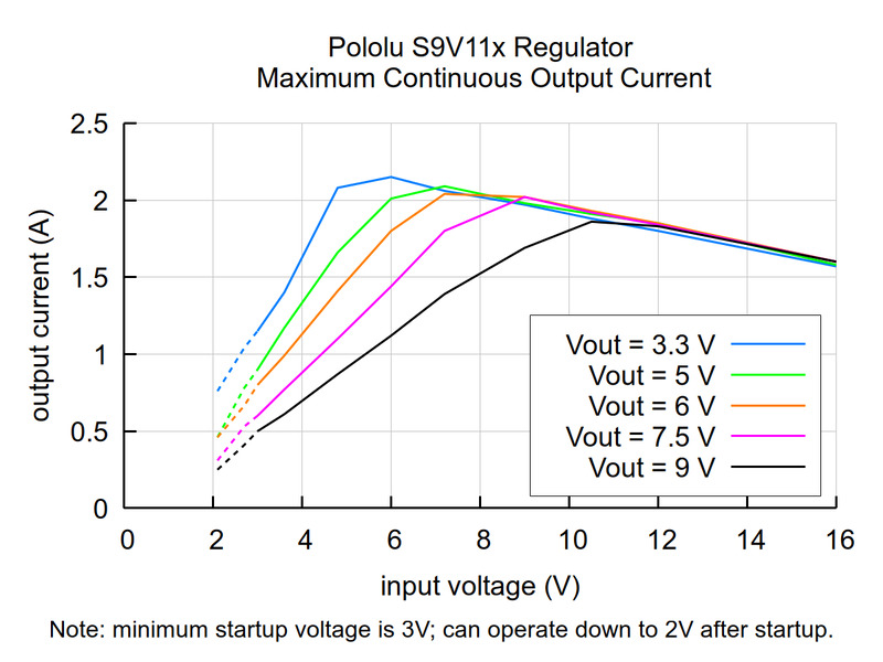 |
Note that the startup current is limited to approximately 700 mA, and currents in excess of this are only available after the output has finished rising to 5 V. Large capacitive loads will generally not pose a problem because they will gradually charge up even with the current limit active, so while they may increase the time it takes the regulator to start up, the regulator should still eventually get to 5 V. A purely resistive load, however, could prevent the regulator from ever reaching 5 V. For example, if you put a 5 Ω resistor between VOUT and GND and then apply power to the regulator, the output voltage will never rise past 3.5 V, the voltage at which the current draw reaches the 700 mA limit. As such, this regulator is intended for applications like robotics, where any large loads are controllable and can be applied only after the regulator has finished starting up.
During normal operation, this product can get hot enough to burn you. Take care when handling this product or other components connected to it.
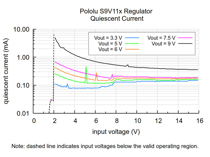
The quiescent current is the current the regulator uses just to power itself, and the graph below shows this as a function of the input voltage. The module’s EN input can be driven low to put the board into a low-power state where it typically draws 10 µA per volt on VIN.
 |
When connecting voltage to electronic circuits, the initial rush of current can cause voltage spikes that are much higher than the input voltage. If these spikes exceed the regulator’s maximum voltage (16 V), the regulator can be destroyed. In our tests with typical power leads (~30″ test clips), we observed spikes approaching 16 V at input voltages approaching 9 V. Power supplies or leads with high inductance will make these spikes worse. An electrolytic capacitor (33 μF is a good starting point) can be added close to the regulator between VIN and GND to help suppress these spikes.
More information about LC spikes can be found in our application note, Understanding Destructive LC Voltage Spikes.
| Size: | 0.5″ × 0.6″ × 0.25″1 |
|---|---|
| Weight: | 0.8 g1 |
| Minimum operating voltage: | 2 V2 |
|---|---|
| Maximum operating voltage: | 16 V |
| Continuous output current: | 1.7 A3 |
| Output voltage: | 5 V4 |
| Reverse voltage protection?: | N |
| Maximum quiescent current: | 0.4 mA5 |
| Low-voltage cutoff: | precision adjustable |
| Output type: | fixed 5V (default), 6V selectable |
| PCB dev codes: | reg20b |
|---|---|
| Other PCB markings: | 0J10534 |
Note: this dimension diagram does not apply to the smaller S9V11F5.
Note: this model does not apply to the smaller S9V11F5.
This DXF drawing shows the locations of all of the board’s holes. Note that this does not apply to the smaller S9V11F5.
No FAQs available.
I am excited to announce our first voltage regulators with multi-turn trimmer potentiometers! I have wanted to add multi-turn pots to our products...