

This is a merged information page for Item #2568.
View normal product page.
Pololu item #:
2568
Brand:
Pololu
Status:
Active

| Output voltage | Typical max input current* | Min input voltage |
|---|---|---|
| 12 V | 5 A | 2.9 V |
*Actual achievable maximum continuous current is a function of input voltage and is limited by thermal dissipation.
Alternatives available with variations in these parameter(s): output voltage Select variant…
 Compare all products in U3V50x Step-Up Voltage Regulators.
|
Pololu step-up voltage regulator U3V50F5, U3V50F6, U3V50F9, and U3V50F12. |
|---|
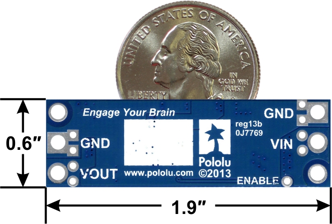 |
Pololu step-up voltage regulator U3V50x, bottom view with dimensions. |
|---|
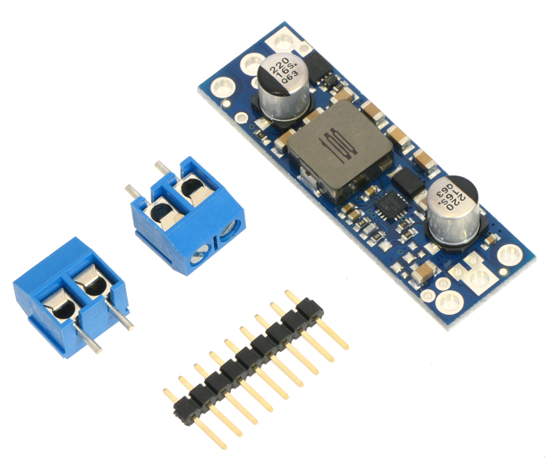 |
Pololu fixed step-up voltage regulator U3V50Fx with included optional terminal blocks and header pins. |
|---|
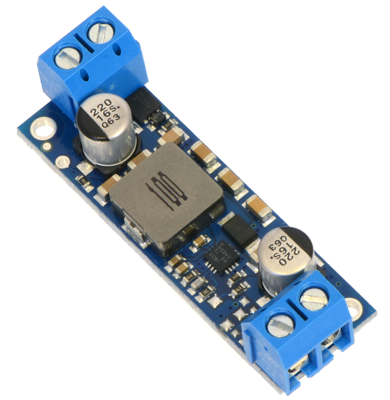 |
Pololu fixed step-up voltage regulator U3V50Fx, assembled with included terminal blocks. |
|---|
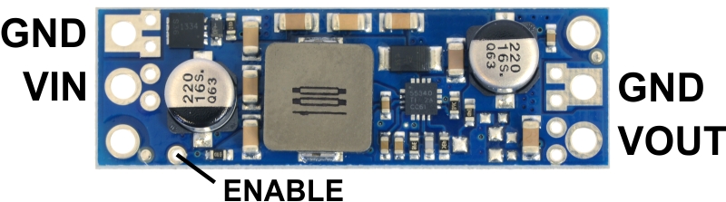 |
Pololu fixed step-up voltage regulator U3V50Fx, labeled top view. |
|---|
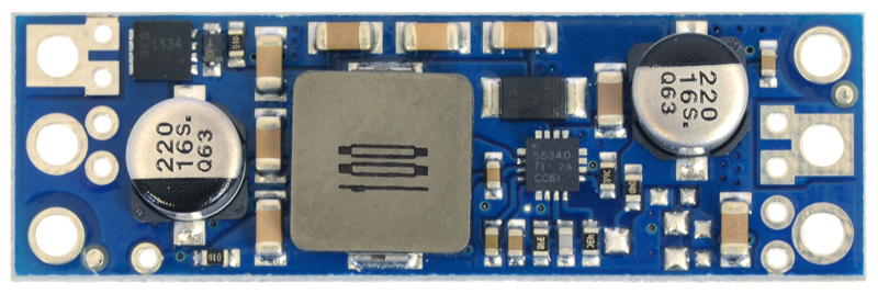 |
Pololu fixed step-up voltage regulator U3V50Fx, top view. |
|---|
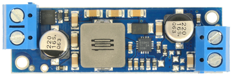 |
Pololu fixed step-up voltage regulator U3V50Fx, assembled with included terminal blocks. |
|---|
 |
Pololu step-up voltage regulator U3V50x with included terminal blocks installed, side view. |
|---|
 |
Typical efficiency of Pololu 5 V step-up voltage regulator U3V50F5. |
|---|
 |
Typical efficiency of Pololu 6 V step-up voltage regulator U3V50F6. |
|---|
 |
Typical efficiency of Pololu 9 V step-up voltage regulator U3V50F9. |
|---|
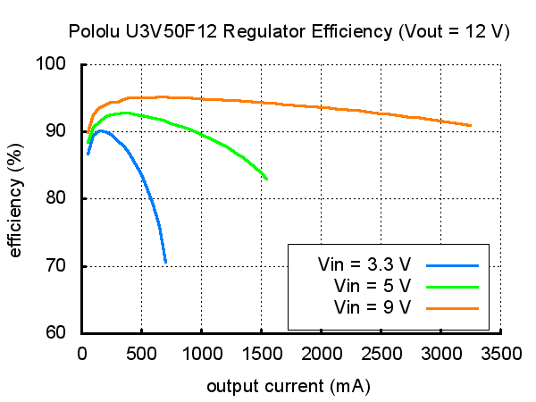 |
Typical efficiency of Pololu 12 V step-up voltage regulator U3V50F12. |
|---|
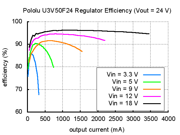 |
Typical efficiency of Pololu 24 V step-up voltage regulator U3V50F24. |
|---|
Note: We recommend our newer U3V70x family of boost regulators over these older U3V50x regulators for applications that require 20 V or less. The U3V70x regulators are smaller and can deliver more current, and the adjustable version features a precision 11-turn potentiometer, which makes it easier to set the output voltage to a particular value.
|
These boost (step-up) voltage regulators generate higher output voltages from input voltages as low as 2.9 V. They are switching regulators (also called switched-mode power supplies (SMPS) or DC-to-DC converters) and have a typical efficiency between 80% to 95%. The available output current is a function of the input voltage, output voltage, and efficiency (see the Typical Efficiency and Output Current section below), but the input current can typically be as high as 5 A. This regulator is available with a fixed 5 V, 6 V, 9 V, 12 V, or 24 V output:
Alternatives available with variations in these parameter(s): output voltage Select variant…
The U3V50x regulator family also includes two adjustable-output versions: the U3V50ALV offers an output range of 4 V to 12 V and the U3V50AHV offers an output range of 9 V to 30 V. The different versions of the board all look very similar, so the bottom silkscreen includes a blank space where you can add your own distinguishing marks or labels.
The no-load quiescent current will typically be between 1 mA and 5 mA for most combinations of input and output voltages, though the combination of a very high output voltage and a very low input voltage (e.g. when boosting from 3 V in to 30 V out) can result in quiescent currents on the order of a few dozen milliamps. The ENABLE pin can be used to put the board in a low-power state that reduces the quiescent current to approximately 20 µA per volt on VIN.
This regulator has built-in reverse-voltage protection, over-current protection, thermal shutdown (which typically activates at 165°C), and an under-voltage lockout that causes the regulator to turn off when the input voltage is below 2.5 V (typical).
This boost regulator has four connections: input voltage (VIN), ground (GND), and output voltage (VOUT), and ENABLE.
|
The input voltage, VIN, must be at least 2.9 V and should not exceed the output voltage, VOUT. (If VIN is higher than VOUT, the higher input voltage will show up on the output, which is potentially dangerous for your connected load and could also damage the regulator.)
The regulator is enabled by default: a 100 kΩ pull-up resistor on the board connects the ENABLE pin to reverse-protected VIN. The ENABLE pin can be driven low (under 0.7 V) to put the board into a low-power state. The quiescent current draw in this sleep mode is dominated by the current in the pull-up resistor from ENABLE to VIN and by the reverse-voltage protection circuit, which will draw between 10 µA and 20 µA per volt on VIN when ENABLE is held low. If you do not need this feature, you should leave the ENABLE pin disconnected. Note that like most boost regulators, the input power will pass through to the output when the board is disabled, so the ENABLE pin cannot be used to turn off power to the load.
|
|
The connections are labeled on the back side of the PCB, and the board offers several options for making electrical connections. The eight smaller through-holes on the ends of the board are arranged with a 0.1″ spacing for compatibility with solderless breadboards, connectors, and other prototyping arrangements that use a 0.1″ grid; you can solder pieces of the included 9×1 straight male header strip into these smaller holes. Alternatively, you can solder the included 2-pin 5mm-pitch terminal blocks to the two pairs of larger holes on the ends of the board. For the most compact installation, you can solder wires directly to the board.
Note that this regulator has a thick PCB (0.093″), so terminal block and header pins will not protrude as far through the holes as they would with typical 0.062″-thick PCBs.
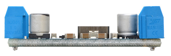 |
Pololu step-up voltage regulator U3V50x with included terminal blocks installed, side view. |
|---|
The board has two mounting holes intended for #2 or M2 screws. The mounting holes are at opposite corners of the board, separated by 1.7″ horizontally and 0.4″ vertically.
The efficiency of a voltage regulator, defined as (Power out)/(Power in), is an important measure of its performance, especially when battery life or heat are concerns. As shown in the graphs below, these switching regulators have an efficiency of 80% to 95% for most combinations of input voltage, output voltage, and load.
|
|
|
|
|
The maximum achievable output current is approximately proportional to the ratio of the input voltage to the output voltage. If the input current exceeds the 5 A switch current limit, the output voltage will begin to drop. Additionally, the maximum output current can depend on other factors, including the ambient temperature, air flow, and heat sinking.
During normal operation, this product can get hot enough to burn you. Take care when handling this product or other components connected to it.
| Size: | 0.6″ × 1.9″ × 0.41″1 |
|---|---|
| Weight: | 7.5 g2 |
| Minimum operating voltage: | 2.9 V |
|---|---|
| Maximum operating voltage: | 12 V |
| Maximum input current: | 5 A |
| Output voltage: | 12 V |
| Reverse voltage protection?: | Y |
| Maximum quiescent current: | 8 mA3 |
| PCB dev codes: | reg13b |
|---|---|
| Other PCB markings: | 0J7769, blank white box |
This DXF drawing shows the locations of all of the board’s holes.
No FAQs available.
Ever since the release of our original adjustable boost regulators, customers have been requesting higher-power versions. Doing power systems right...