

This is a merged information page for Item #2483.
View normal product page.
Pololu item #:
2483
Brand:
Pololu
Status:
Active and Preferred

The Pololu basic relay carrier modules allow simple control of a single-pole, double-throw (SPDT) switch from low-voltage, low-current control signals. This item includes the basic carrier PCB along with an Omron G5LE-14-DC12 12 V relay, 5.0 mm terminal blocks, and 0.1″ male headers in straight and right-angle versions. Surface-mount components are pre-assembled on the PCB, but the through-hole components are not installed. The included power relay is rated for up to 10 A under most conditions.
Alternatives available with variations in these parameter(s): channels voltage style Select variant…
 Compare all products in Relay Modules.
|
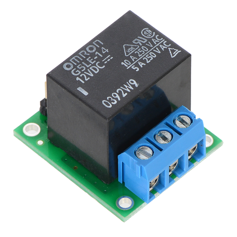
Pololu basic SPDT relay carrier with 12 VDC relay (partial kit). |
|---|
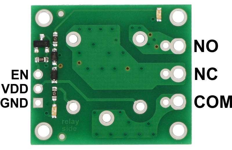 |
Pinout of Pololu basic SPDT relay carrier for “sugar cube” relays. |
|---|
 |
Pololu basic SPDT relay carrier with 12 VDC relay (assembled). |
|---|
 |
Pololu basic SPDT relay carrier with 12 VDC relay (assembled). |
|---|
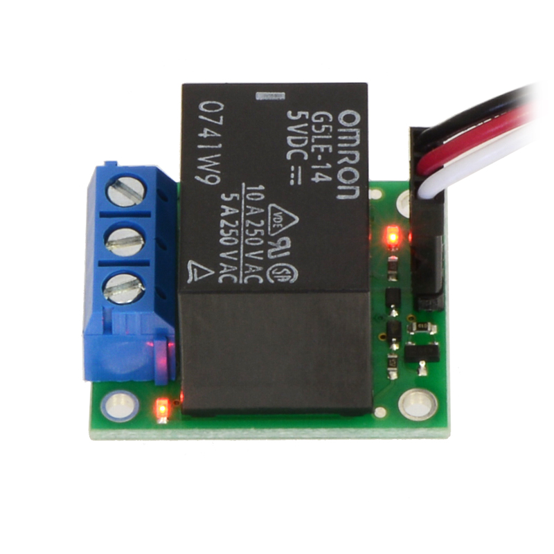 |
Pololu basic SPDT relay carrier with relay energized (servo cable not included). |
|---|
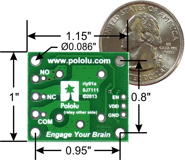 |
Pololu basic SPDT relay carrier with dimensions. |
|---|
 |
Schematic diagram for the Pololu basic SPDT relay carriers. |
|---|
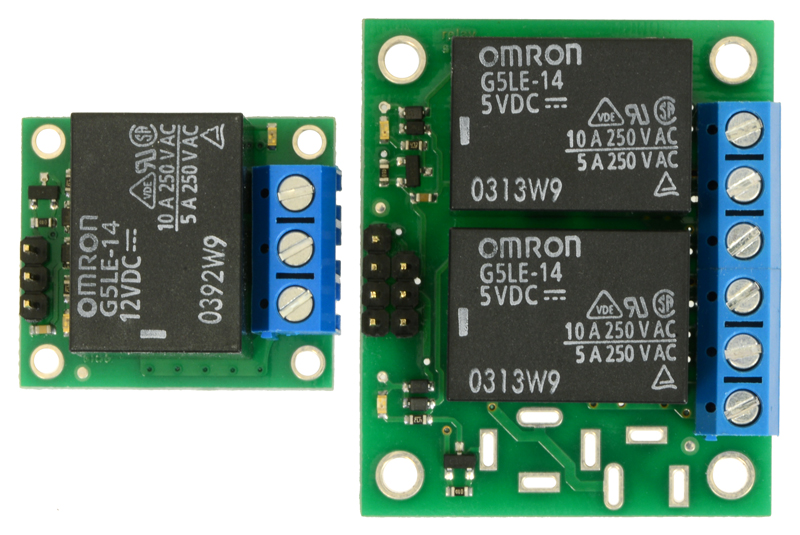 |
Side-by-side comparison of the single and dual versions of the Pololu basic SPDT relay carriers. |
|---|
The Pololu basic relay carrier modules make it easy to control electrically isolated, single-pole, double-throw (SPDT) switches from low-voltage, low-current control signals. The modules are available in single-channel and dual-channel versions with 5 V or 12 V power relays—Omron G5LE-14-DC5 and G5LE-14-DC12 (1MB pdf), respectively—and with a variety of connector and assembly options.
The following table lists the available Pololu basic SPDT relay carrier options:
| Channels | Board size | Mounting holes |
DC power jack option |
Relay coil voltage |
Coil resistance |
Active current at rated voltage |
Connector and assembly options | Item # | Price | |
|---|---|---|---|---|---|---|---|---|---|---|
 Single-relay RC interface |
1 | 1.35″ × 1.0″ | 4× 0.086″ (#2 or M2) |
no | 5 V | 63 Ω | 80 mA | • with all through-hole parts soldered | 2804 | $17.95 |
| • through-hole parts included but not soldered | 2805 | $15.95 | ||||||||
 Single-relay digital enable |
1 | 1.15″ × 1.0″ | 4× 0.086″ (#2 or M2) |
no | 5 V | 63 Ω | 80 mA | • with JST SH-style connector, assembled | 5662 | $7.95 |
| • with 0.1″ headers, assembled | 2480 | $7.95 | ||||||||
| • with 0.1″ headers, partial kit | 2481 | $6.95 | ||||||||
| 12 V | 360 Ω | 34 mA | • with JST SH-style connector, assembled | 5663 | $7.95 | |||||
| • with 0.1″ headers, assembled | 2482 | $7.95 | ||||||||
| • with 0.1″ headers, partial kit | 2483 | $6.95 | ||||||||
| N/A | N/A | N/A | • carrier board with JST SH-style connector only (no relay) | 5664 | $3.95 | |||||
| • carrier board only (no relay or connectors) | 2479 | $3.95 | ||||||||
 Dual-relay digital enable |
2 | 1.5″ × 1.8″ | 4× 0.125″ (#4 or M3) |
yes | 5 V | 63 Ω | 80 mA | • with JST SH-style connector, assembled | 5665 | $14.95 |
| • with 0.1″ headers, assembled | 2485 | $14.95 | ||||||||
| • with 0.1″ headers, partial kit | 2486 | $13.49 | ||||||||
| 12 V | 360 Ω | 34 mA | • with JST SH-style connector, assembled | 5666 | $14.95 | |||||
| • with 0.1″ headers, assembled | 2487 | $14.95 | ||||||||
| • with 0.1″ headers, partial kit | 2488 | $13.49 | ||||||||
| N/A | N/A | N/A | • carrier board with JST SH-style connector only (no relays) | 5667 | $7.49 | |||||
| • carrier board only (no relays or connectors) | 2484 | $6.95 | ||||||||
Alternatives available with variations in these parameter(s): channels voltage style Select variant…
|
|
This carrier version is partial kit that includes:
Either of the header strips can be broken or cut into a 1×3 section and soldered into the three control through-holes. These headers are compatible with solderless breadboards, 0.1″ jumper wires, and female servo cables.
For the switch connections, you can take the remaining 1×5 strip and remove every other pin to make a 0.2″-pitch header that can be soldered to the smaller holes on that side of the board, or you can solder the included 5mm-pitch terminal block to the larger holes. The following pictures show a unit assembled with straight headers and terminal blocks:
|
|
|
|
The switch portion of the relay (NO, NC, and COM) is accessible on one side of the board via larger holes that work with the included 5mm-pitch terminal block or smaller holes that work with 0.2″ headers. The control pins (EN, VDD, GND) are routed to the 0.1″-pitch through-holes on the other side of the board that work with the included 0.1″ straight and right-angle headers. The 12 V relay coil is powered by supplying 12 V across the VDD and GND pins, and it is activated by a digital high (2.5 V to 20 V) control signal on the EN pin. The control signal is fed directly to a BSS138K N-channel MOSFET, which in turn actuates the relay coil when the control voltage exceeds approximately 2.5 V, up to a maximum of 20 V (see BSS138K datasheet (517k pdf) for details). Red LEDs on either side of the relay light up when the relay coil is active. The carrier board has four mounting holes that work with #2 or M2 screws.
The relay switch terminals COM (common), NO (normally open), and NC (normally closed) are routed on the PCB with a minimum clearance/creepage of 60 mil (1.5 mm) from other copper. The copper traces are designed to be at least 45 mil (1.1 mm) from the board edges, though manufacturing variations in the board edges can make those distances slightly lower.
In most applications, the current and voltage ratings for the module will match the ratings of the relay used. Maximum current, maximum voltage, and life expectancy are interdependent; we therefore recommend careful examination of your relay’s datasheet.
Warning: This product is not designed to or certified for any particular high-voltage safety standard. Working with voltages above 30 V can be extremely dangerous and should only be attempted by qualified individuals with appropriate equipment and protective gear.
|
Schematic diagram for the Pololu basic SPDT relay carriers. |
|---|
This schematic is also available as a downloadable pdf (119k pdf).
| Size: | 1″ × 1.15″ × 0.1″1 |
|---|---|
| Weight: | 16 g |
| Channels: | 1 |
|---|---|
| Voltage: | 12 V |
| Partial kit?: | Y |
| Style: | partial kit (relays, 0.1″ headers, and 5mm terminal blocks included but not soldered in) |
| PCB dev codes: | 0J7111 |
|---|---|
| Other PCB markings: | 0J7111, 0J7194 |
This DXF drawing shows the locations of all of the board’s holes.
No FAQs available.
No blog posts to show.