LSM303DLM 3D Compass and Accelerometer Carrier with Voltage Regulators

The LSM303DLM combines a digital 3-axis accelerometer and 3-axis magnetometer into a single package that is ideal for making a tilt-compensated compass. The six independent readings, whose sensitivities can be set in the ranges of ±2 to ±8 g and ±1.3 to ±8.1 gauss, are available through an I²C interface. The carrier board operates from 2.6 to 5.5 V and has a 0.1″ pin spacing.
| Description | Specs (7) | Pictures (5) | Resources (7) | FAQs (1) | On the blog (1) | Distributors (0) |
|---|
Discontinuation notice: This board has been replaced by the newer LSM303D carrier, which offer improved magnetic sensing resolution, a wider acceleration measurement range, and the option of using an SPI interface rather than I²C. The LSM303D carrier is not pin-compatible with earlier LSM303 carriers.
 |
Overview
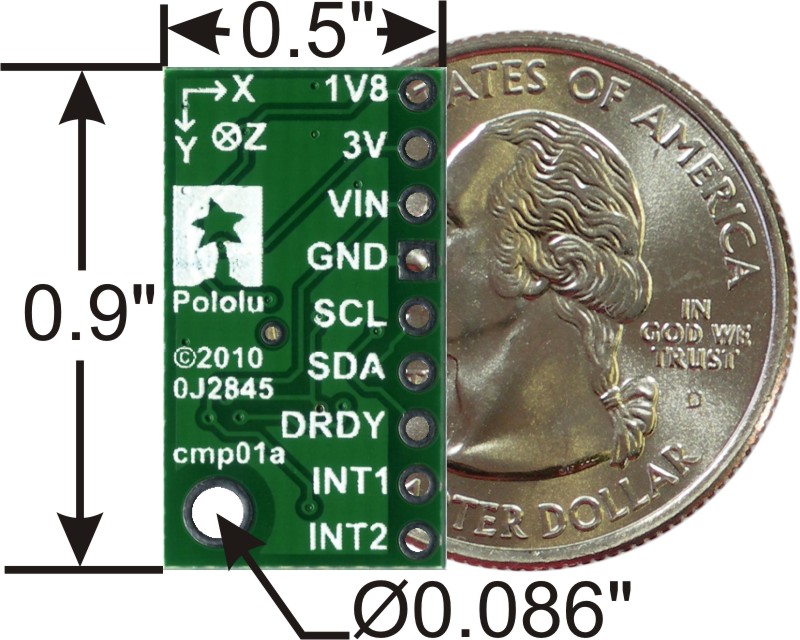
This board is a compact (0.5" × 0.9") breakout board for ST’s LSM303DLM 3-axis accelerometer and 3-axis magnetometer; we therefore recommend careful reading of the LSM303DLM datasheet (519k pdf) before using this product. The LSM303DLM is a great IC, but its small package makes it difficult for the typical student or hobbyist to use. The device also requires multiple voltage supplies not typically available when interfacing with 3.3 or 5 V systems. This carrier board addresses these issues by incorporating additional electronics, including two voltage regulators and a level-shifting circuit, while keeping the overall size as compact as possible. The board ships fully populated with its SMD components, including the LSM303DLM, as shown in the product picture.
The LSM303DLM has many configurable options, including dynamically selectable sensitivities for the accelerometer and magnetometer, a choice of output data rates, and two independently-programmable external inertial interrupt pins. The magnetometer and accelerometer can be individually turned on and off to save power, and a special sleep-to-wakeup function allows the accelerometer to sleep until an inertial interrupt is triggered. The six independent magnetic and acceleration readings (sometimes called 6DOF) are available through an I²C/TWI interface and can be used for many applications, including making a tilt-compensated compass that can be used to determine headings regardless of how the board is inclined (ST provides an application note (1MB pdf) that explains the details of making one).
The carrier board includes two voltage regulators that provide the 1.8 V and 3 V required by the LSM303DLM, which allows the sensor to be powered from a single 2.6 – 5.5 V supply. The regulator outputs are available on the 1V8 and 3V pins and can supply almost 150 mA and 300 mA, respectively, to external devices. The breakout board also includes a circuit that shifts the I²C clock and data lines to the same logic voltage level as the supplied VIN, making it simple to interface the board with 3.3 V or 5 V systems, and the board’s 0.1" pin spacing makes it easy to use with standard solderless breadboards and 0.1" perfboards.
For sensor fusion applications, our MinIMU-9 v3 and AltIMU-10 v4 inertial measurement units combine the similar LSM303D accelerometer/magnetometer with an L3GD20H 3-axis gyro on a single board, providing nine independent readings that can be used to calculate an absolute orientation. The AltIMU-10 v4 also includes an LPS25H pressure sensor that can be used to calculate altitude.
Specifications
- Dimensions: 0.5" × 0.9" × 0.1" (13 × 23 × 3 mm)
- Weight without header pins: 0.84 g (0.03 oz)
- Operating voltage: 2.6 to 5.5 V
- Supply current: 10 mA
- Output format (I2C):
- Accelerometer: one 12-bit reading (left-justified) per axis
- Magnetometer: one 12-bit reading (right-justified) per axis
- Sensitivity range (configurable):
- Accelerometer: ±2, ±4, or ±8 g
- Magnetometer: ±1.3, ±1.9, ±2.5, ±4.0, ±4.7, ±5.6, or ±8.1 gauss
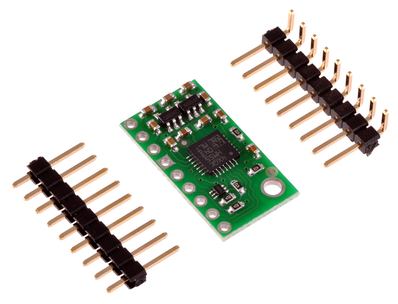
Included components
A 9×1 strip of 0.1" header pins and a 9×1 strip of 0.1" right-angle header pins are included, as shown in the picture below. You can solder the header strip of your choice to the board for use with custom cables or solderless breadboards, or you can solder wires directly to the board itself for more compact installations.
 |
Using the LSM303DLM
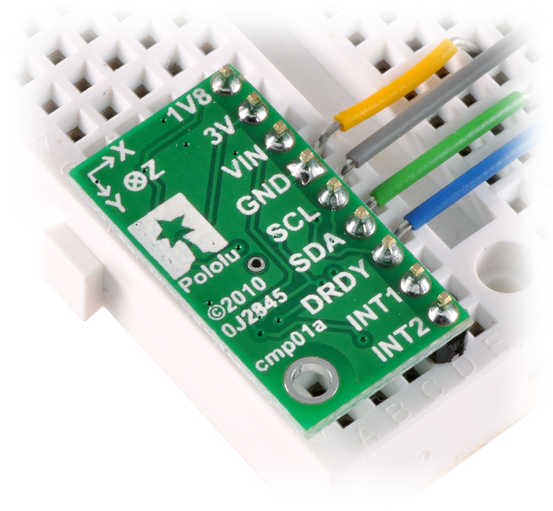
Connections
A minimum of four connections are necessary to use the LSM303DLM: VIN, GND, SCL, and SDA. VIN should be connected to a 2.6 – 5.5 V source, GND to 0 volts, and SCL and SDA should be connected to an I²C bus operating at the same logic level as VIN.
|
|

Pinout
| PIN | Description |
|---|---|
| VIN | This is the main 2.6 – 5.5 V power supply connection. The SCL and SDA level shifters pull the I²C bus high bits up to this level. |
| GND | The ground (0 V) connection for your power supply. Your I²C control source must also share a common ground with this board. |
| 1V8 | Regulated 1.8 V output. Almost 150 mA is available to power external components. |
| 3V | Regulated 3.0 V output. Almost 300 mA is available to power external components. |
| SCL | Level-shifted I²C clock line: HIGH is VIN, LOW is 0 V |
| SDA | Level-shifted I²C data line: HIGH is VIN, LOW is 0 V |
| DRDY | Magnetometer data ready indicator, a 1.8V-logic-level output. HIGH (1.8 V) indicates magnetometer data can be read. LOW (0 V) indicates the magnetometer is writing new data to the data registers. This output is not level-shifted. |
| INT1 | Inertial interrupt 1, a 1.8V-logic-level output. This output is not level-shifted. |
| INT2 | Inertial interrupt 2, a 1.8V-logic-level output. This output is not level-shifted. |
Schematic Diagram
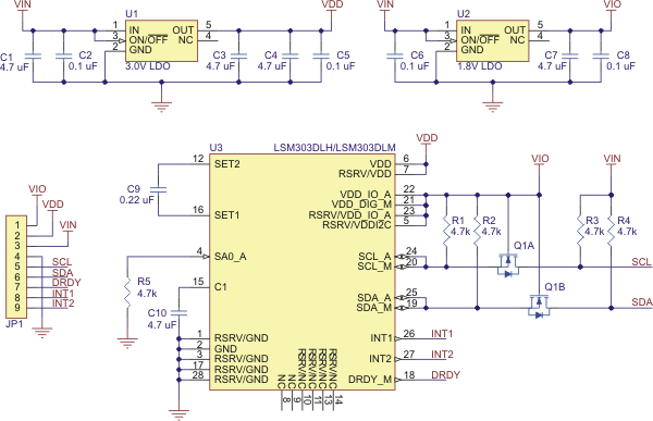 |
The above schematic shows the additional components the carrier board incorporates to make the LSM303DLM easier to use, including the voltage regulators that allow the board to be powered from a single 2.6 – 5.5 V supply and the level-shifter circuit that allows for I²C communication at the same logic voltage level as VIN.
I²C Communication
The LSM303DLM readings can be queried and the device can be configured through the I²C bus. The module acts as two chained I²C slave devices, with the accelerometer and magnetometer clock and data lines tied together to the same I²C bus to ease communication. Additionally, level shifters on the I²C clock (SCL) and data lines (SDA) enable I²C communication with microcontrollers operating at the same voltage as VIN (2.6 – 5.5V). A detailed explanation of the protocol can be found in the LSM303DLM datasheet (519k pdf), and more detailed information about I²C in general can be found in NXP’s I²C-bus specification (1MB pdf).
The accelerometer and the magnetometer have separate 7-bit slave addresses on the I²C bus. The magnetometer’s slave address is 0011110b and cannot be changed. The accelerometer’s slave address has its least significant bit (LSb) determined by the voltage on the slave address selector pad (SA0_A). The carrier board pulls SA0_A to ground through a 4.7kΩ resistor, setting the accelerometer’s slave address to 0011000b by default. If the accelerometer’s selected slave address happens to conflict with some other device on your I²C bus, it is possible to access SA0_A through the untented via on the bottom of the board and pull it up.
In our tests of the board, we were able to communicate with the chip at clock frequencies up to 400 kHz; higher frequencies might work but were not tested. The chip itself and carrier board do not meet of some requirements to make the device compliant with I²C fast-mode. It is missing 50ns spike suppression on the clock and data lines, and additional pull-ups on the clock and data lines might also be necessary to achieve compliant signal timing characteristics.
Sample Code
- Arduino/A-Star: We have written a basic Arduino library for this LSM303 carrier board that makes it easy to interface this sensor with an Arduino or Arduino-compatible board like an A-Star. The library makes it simple to read the raw accelerometer and magnetometer data, and it has a function for computing the tilt-compensated heading for those looking to use this sensor as a tilt-compensated compass.
- Orangutans: We provide an AVR Studio project (5k zip) that demonstrates how to use an Orangutan robot controller to interface with the LSM303DLM and make a tilt-compensated compass. The project is set up for an ATmega328P microcontroller, but it will work on other Orangutans with simple changes to the project configuration.
- mbed: There is a library for using the similar LSM303DLH with the ARM mbed development board. This library was not written and is not maintained by Pololu, and it needs to be modified slightly to work with the LSM303DLM.
Protocol Hints
The datasheet provides all the information you need to use this sensor, but picking out the important details can take some time. Here are some pointers for communicating with and configuring the LSM303DLM that we hope will get you up and running a little bit faster:
- The magnetometer and accelerometer are off by default. You have to turn them on by setting the correct configuration registers.
- The magnetometer will not update its data until all 6 data bytes have been read during a single I²C transfer. All the bytes can be read in the same transfer using the the magnetometer’s automatic subaddress updating feature (this feature is enabled by default).
- The accelerometer also has an automatic subaddress updating feature, if you assert the most significant bit of the subaddress. The accelerometer does not require you to read all of the output bytes before updating by default.
- The accelerometer and magnetometer combined in this IC are made by separate manufacturers, so there are fairly significant differences in their features, functionality, and interfaces.
Inertial Interrupts
The inertial interrupts (INT1 and INT2) are highly configurable 1.8V-level outputs that can change due to accelerations (the magnetometer has no effect on INT1 or INT2). If the sleep-to-wakeup feature of the accelerometer is enabled, when an interrupt is triggered, the accelerometer wakes up.
Related products


Home | Forum | Blog | Support | Ordering Information | Lists | Distributors | BIG Order Form | About | Contact
© 2001–2026 Pololu Corporation
