

This is a merged information page for Item #2115.
View normal product page.
Pololu item #:
2115
Brand:
Pololu
Status:
Obsolete

The compact (0.32″×0.515″) U3V12F5 switching step-up (or boost) voltage regulator takes an input voltage as low as 2.5 V and efficiently boosts it to 5 V. The pins have a 0.1″ spacing, making this board compatible with standard solderless breadboards and perfboards.
Alternatives available with variations in these parameter(s): output voltage Select variant…
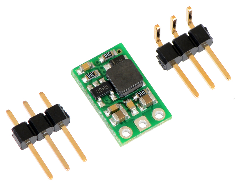 |
Pololu step-up voltage regulator U3V12Fx with included hardware. |
|---|
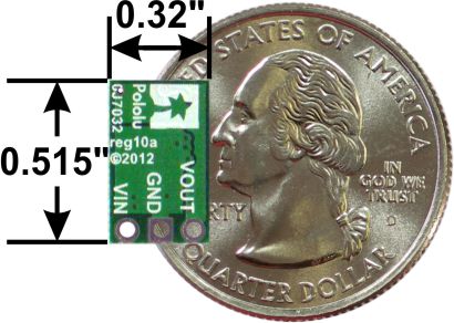 |
Pololu step-up voltage regulator U3V12Fx, bottom view with dimensions. |
|---|
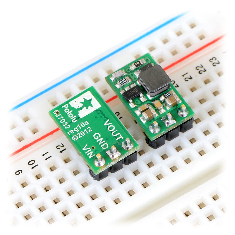 |
Pololu step-up voltage regulators U3V12Fx in a breadboard. |
|---|
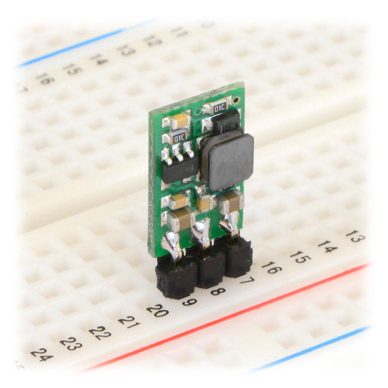 |
Pololu step-up voltage regulator U3V12Fx in a breadboard. |
|---|
 |
Typical efficiency of Pololu step-up voltage regulator U3V12F5. |
|---|
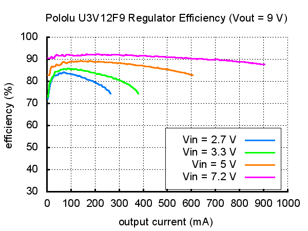 |
Typical efficiency of Pololu step-up voltage regulator U3V12F9. |
|---|
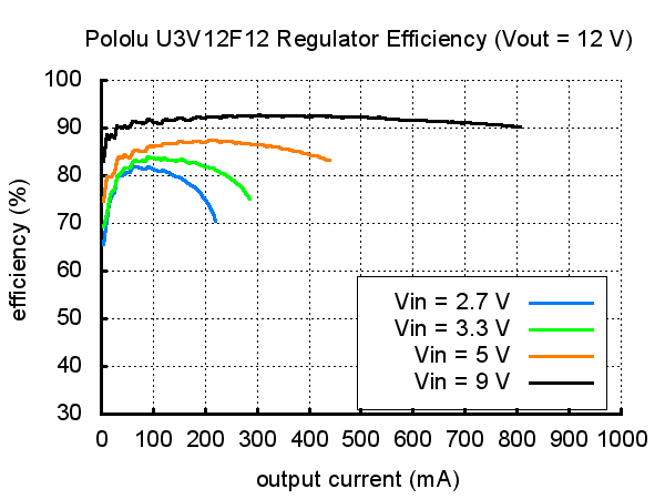 |
Typical efficiency of Pololu step-up voltage regulator U3V12F12. |
|---|
Note: The U3V12Fx family of voltage regulators has been discontinued due to key components becoming obsolete. For alternatives, please consider the U3V9Fx Step-Up Voltage Regulator family, which should work as a drop-in replacements in most applications.
|
These boost (step-up) voltage regulators generate higher output voltages from input voltages as low as 2.5 V. They are switching regulators (also called switched-mode power supplies (SMPS) or DC-to-DC converters) and have a typical efficiency between 80% to 90%. The available output current is a function of the input voltage, output voltage, and efficiency (see Typical Efficiency and Output Current section below), but the input current can typically be as high as 1.4 A. This regulator is available with a fixed 5 V, 9 V, or 12 V output:
Alternatives available with variations in these parameter(s): output voltage Select variant…
The regulator’s thermal shutdown prevents damage from overheating, but it does not have short-circuit or reverse-voltage protection.
|
|
The boost regulator has three connections: input voltage (VIN), ground (GND), and output voltage (VOUT).
The input voltage, VIN, must be at least 2.5 V and should not exceed the output voltage, VOUT. Please be wary of destructive LC spikes that might cause the input voltage to exceed VOUT (see below for more information).
The three connections are labeled on the back side of the PCB, and they are arranged with a 0.1″ spacing along the edge of the board for compatibility with solderless breadboards, connectors, and other prototyping arrangements that use a 0.1″ grid. You can solder wires directly to the board or solder in either the 3×1 straight male header strip or the 3×1 right-angle male header strip that is included.
|
The efficiency of a voltage regulator, defined as (Power out)/(Power in), is an important measure of its performance, especially when battery life or heat are concerns. As shown in the graphs below, this switching regulator typically has an efficiency of 80 to 90%.
|
|
|
The maximum achievable output current is approximately proportional to the ratio of the input voltage to the output voltage. If the input current exceeds the switch current limit (typically somewhere between 1.4 and 2 A), the output voltage will begin to drop. Additionally, the maximum output current can depend on other factors, including the ambient temperature, air flow, and heat sinking.
When connecting voltage to electronic circuits, the initial rush of current can cause damaging voltage spikes that are much higher than the input voltage. In our tests with typical power leads (~30″ test clips), input voltages above 10 V caused voltage spikes in excess of 20 V. You can suppress such spikes by soldering a 33μF or larger electrolytic capacitor close to the regulator between VIN and GND.
More information about LC spikes can be found in our application note, Understanding Destructive LC Voltage Spikes.
| Size: | 0.32″ × 0.515″ × 0.1″1 |
|---|---|
| Weight: | 0.4 g1 |
| Minimum operating voltage: | 2.5 V |
|---|---|
| Maximum operating voltage: | 5 V |
| Maximum input current: | 1.4 A2 |
| Output voltage: | 5 V |
| Reverse voltage protection?: | N |
| Maximum quiescent current: | 2 mA |
| PCB dev codes: | reg10a |
|---|---|
| Other PCB markings: | 0J7032 |
This DXF drawing shows the locations of all of the board’s holes.
No FAQs available.
No blog posts to show.