

This is a merged information page for Item #2095.
View normal product page.
Pololu item #:
2095
Brand:
Pololu
Status:
Obsolete

This switching regulator uses the SEPIC topology to produce 9 V from input voltages between 2.5 V and 18 V. The wide input range coupled with its ability to convert both higher and lower input voltages makes it useful for applications where the power supply voltage can vary greatly, as with batteries that start above but discharge below 9 V. The compact (0.4″ × 0.575″) module can supply over 300 mA in typical applications.
Alternatives available with variations in these parameter(s): output voltage Select variant…
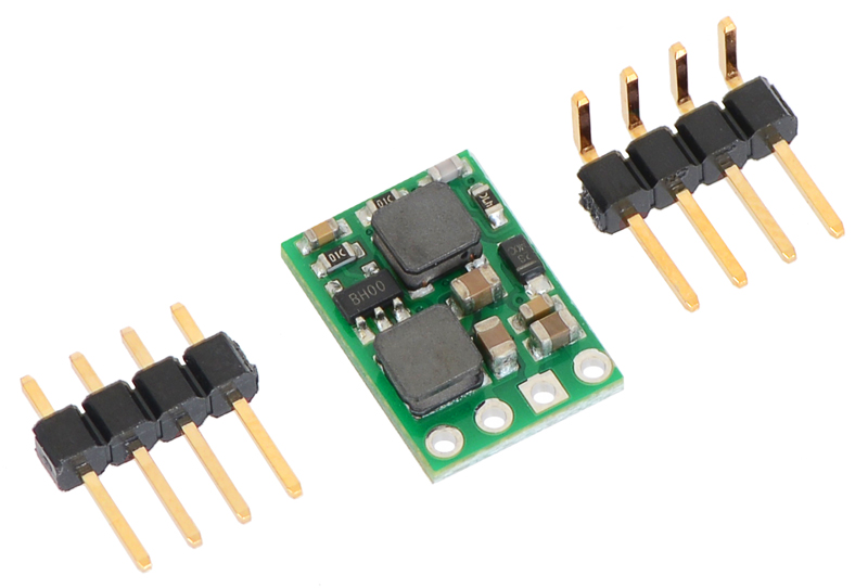 |
Pololu fixed-output step-up/step-down voltage regulator S10VxFx with included optional header pins. |
|---|
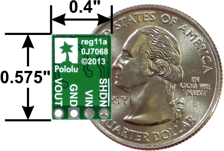 |
Pololu 5V, 9V, and 12V step-up/step-down voltage regulators S10V4F5, S10V3F9, and S10V2F12: bottom view with dimensions. |
|---|
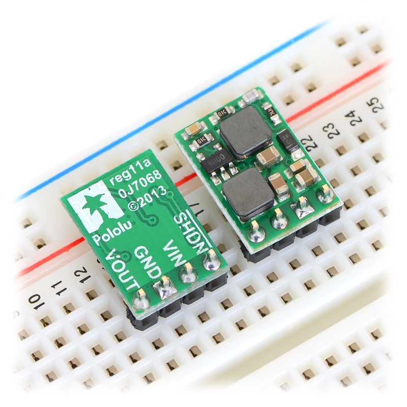 |
Pololu fixed-output step-up/step-down voltage regulators S10VxFx in a breadboard. |
|---|
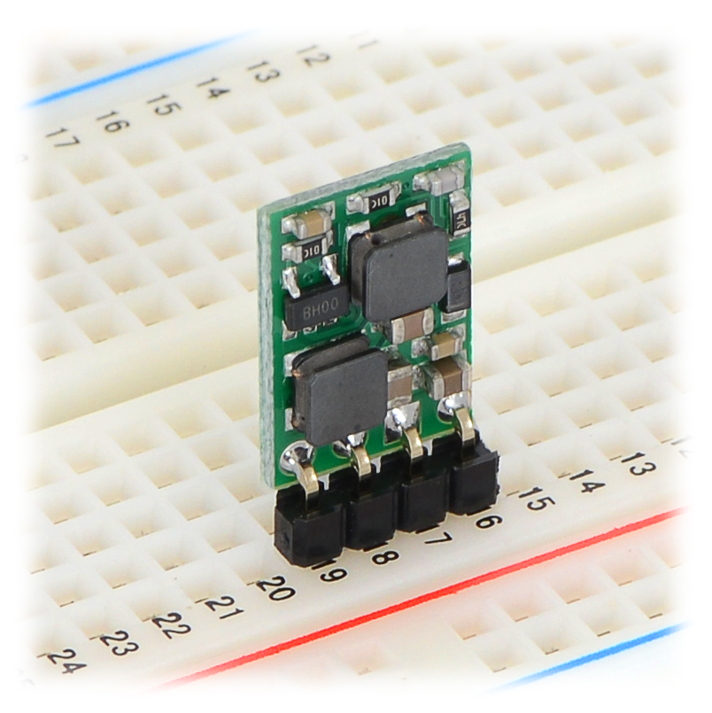 |
Pololu fixed-output step-up/step-down voltage regulator S10VxFx in a breadboard. |
|---|
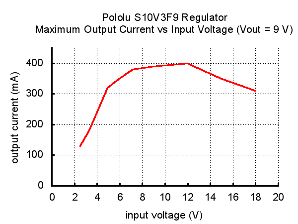 |
Typical maximum output current of Pololu 9V step-up/step-down voltage regulator S10V3F9. |
|---|
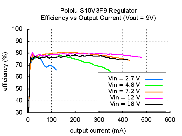 |
Typical efficiency of Pololu 9V step-up/step-down voltage regulator S10V3F9 vs output current. |
|---|
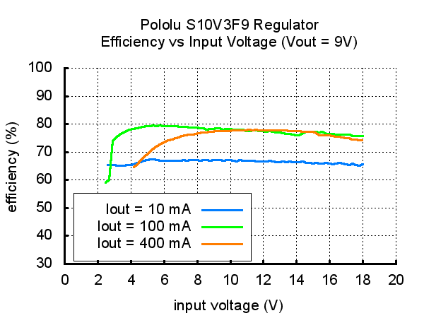 |
Typical efficiency of Pololu 9V step-up/step-down voltage regulator S10V3F9 vs input voltage. |
|---|
|
The Pololu step-up/step-down voltage regulator S10V3F9 is a switching regulator (also called a switched-mode power supply (SMPS) or DC-to-DC converter) with a single-ended primary-inductor converter (SEPIC) topology. It takes an input voltage from 2.5 V to 18 V and increases or decreases the voltage to a fixed 9 V output with a typical efficiency of 70% to 80%.
This flexibility in input voltage is especially well-suited for battery-powered applications in which the battery voltage begins above 9 V and drops below as the battery discharges. Since it lacks the typical restriction that the battery voltage stay above the required voltage throughout its life, new battery packs and form factors can be considered. For instance, a 7-cell battery holder, which might have an 11 V output with fresh alkalines but an 8.4 V nominal voltage with NiMH cells and a 7 V output with partially discharged cells, can now be used to produce a steady 9 V output.
In typical applications, this regulator can deliver over 300 mA continuous; please see the graphs at the bottom of this page for a more detailed characterization. The regulator’s thermal shutdown prevents damage from overheating, but it does not have short-circuit or reverse-voltage protection.
|
|
This regulator is also available with a fixed 5 V output or a fixed 12 V output.
During normal operation, this product can get hot enough to burn you. Take care when handling this product or other components connected to it.
This step-up/step-down regulator has four connections: shutdown (SHDN), input voltage (VIN), ground (GND), and output voltage (VOUT).
The SHDN pin can be driven low (under 0.4 V) to power down the regulator. The quiescent current in this shutdown mode is dominated by the current in the 10 kΩ pull-up resistor from SHDN to VIN. With SHDN held low, this resistor will draw 0.1 mA per volt on VIN (for example, the shutdown current with a 5 V input will be 0.5 mA). This pin should only ever be driven low or left floating; this can be accomplished with a physical switch that toggles it between ground and disconnected, or electrically with something like a transistor controlled by an I/O line.
The input voltage should be between 2.5 V and 18 V. Lower inputs can shut down the voltage regulator; higher inputs can destroy the regulator, so you should ensure that noise on your input is not excessive and be wary of destructive LC spikes (see below for more information).
The four connections are labeled on the back side of the PCB, and they are arranged with a 0.1″ spacing along the edge of the board for compatibility with standard solderless breadboards and perfboards and connectors that use a 0.1″ grid. You can solder wires directly to the board or solder in either the 4×1 straight male header strip or the 4×1 right-angle male header strip that is included.
|
The efficiency of a voltage regulator, defined as (Power out)/(Power in), is an important measure of its performance, especially when battery life or heat are concerns. As shown in the graphs below, this switching regulator typically has an efficiency of 70% to 80%.
|
|
The maximum achievable output current of the board varies with the input voltage but also depends on other factors, including the ambient temperature, air flow, and heat sinking. The graph below shows output currents at which this voltage regulator’s over-temperature protection typically kicks in after a few seconds. These currents represent the limit of the regulator’s capability and cannot be sustained for long periods, so the continuous currents that the regulator can provide are typically lower.
|
When connecting voltage to electronic circuits, the initial rush of current can cause voltage spikes that are much higher than the input voltage. If these spikes exceed the regulator’s maximum voltage, the regulator can be destroyed. In our tests with typical power leads (~30" test clips), input voltages above 11 V caused spikes over 18 V. You can suppress such spikes by soldering a 33 μF or larger electrolytic capacitor close to the regulator between VIN and GND.
More information about LC spikes can be found in our application note, Understanding Destructive LC Voltage Spikes.
| Size: | 0.4″ × 0.575″ × 0.1″1 |
|---|---|
| Weight: | 0.6 g1 |
| Minimum operating voltage: | 2.5 V |
|---|---|
| Maximum operating voltage: | 18 V |
| Maximum output current: | 300 mA2 |
| Output voltage: | 9 V |
| Reverse voltage protection?: | N |
| Maximum quiescent current: | 2 mA3 |
| PCB dev codes: | reg11a |
|---|---|
| Other PCB markings: | 0J7068 |
This DXF drawing shows the locations of all of the board’s holes.
No FAQs available.
No blog posts to show.